Sip system-integration IC chip package and manufacturing method thereof
- Summary
- Abstract
- Description
- Claims
- Application Information
AI Technical Summary
Benefits of technology
Problems solved by technology
Method used
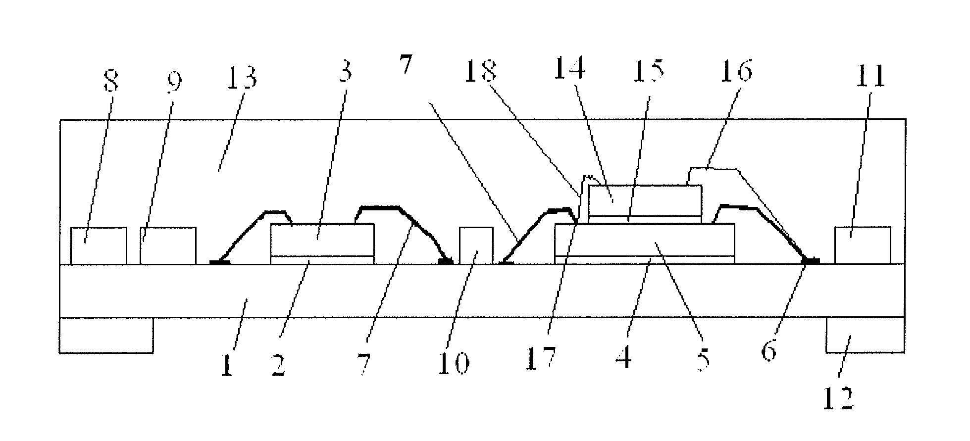
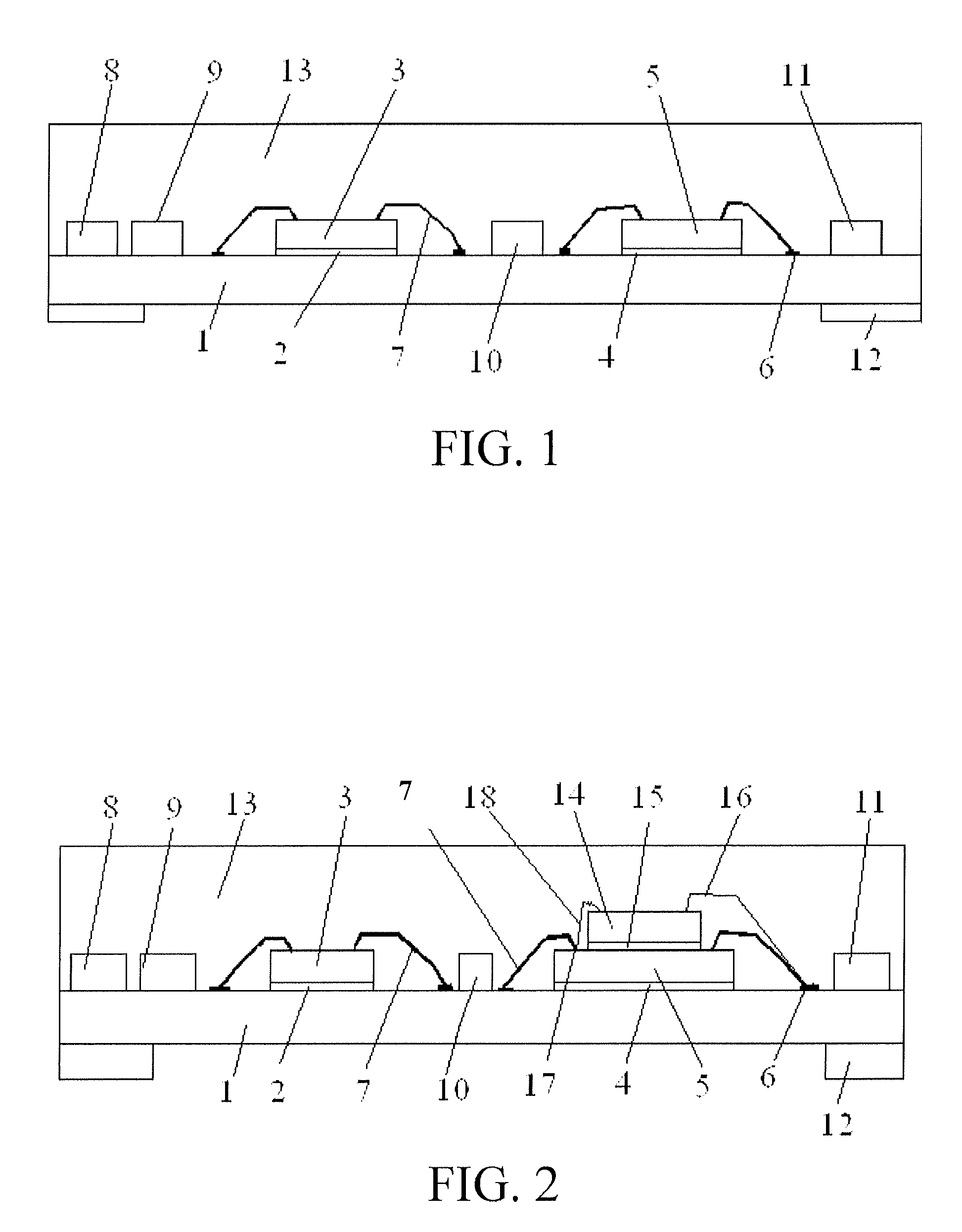
Image

Examples
embodiment 1
[0082]The wafer grinding requires the thickness being less than or equal to 160 μm, so a PG300RM grinding machine and the conventional grinding process are used to perform wafer grinding on a chip. A CP9021B-200 dedicated grinding adhesive film with the specification being 230 mm×100 m and the thickness being 200 μm is adopted, and grinding is performed on a surface of the dedicated grinding adhesive film by using the conventional processes of rough grinding, fine grinding, and polishing, so that the surface roughness of the dedicated grinding adhesive film becomes 0.05 μm-0.12 μm, and the dedicated grinding adhesive film after grinding is adhered to a surface of the chip after wafer grinding. Perform wafer sawing with a DFD3350 dual-blade dicing saw to prevent fragments, and bake after wafer sawing by using an oven of model ESPEC. A substrate adopting an SMT PAD window-opening manner, with the specification of 0201: non-solder mask define and 0402: solder mask define, is used, 96.5...
embodiment 2
[0084]The wafer grinding requires the thickness being greater than 160 μm, so a PG300RM grinding machine and the conventional grinding process are used to perform wafer grinding on a chip. A BT-150E-KL dedicated grinding adhesive film with the specification being 230 mm×100 m and the thickness being 200 μm is adopted, and grinding is performed on a surface of the dedicated grinding adhesive film by using the conventional process, so that the surface roughness of the dedicated grinding adhesive film becomes 0.05 μm-0.12 μm, and the dedicated grinding adhesive film after grinding is adhered to a surface of the chip after wafer grinding. Perform wafer sawing with a DAD6340 dicing saw to prevent fragments, and bake after wafer sawing by using an oven of model ESPEC. A substrate adopting an SMT PAD window-opening manner, with the specification of 0201: non-solder mask define and 0402: solder mask define, is used. 96.5SN 3AG 0.5CU solder paste manufactured by the SENJU is used, a resistor...
embodiment 3
[0086]In a multi-layer stacked package, a lower-layer chip is ground to the thickness of 100 μm-150 μm, and an upper-layer chip is grounded to the thickness of 75 μm-120 μm, a grinding machine has a function of 8″-12″ super-thin grinding and polishing, and uses an anti-warping thin-grinding and thin-polishing process. The taping, cutting, chip mounting and reflow soldering the same as those in Embodiment 1 are used, the cleaning temperature after the reflow soldering is 40° C., and perform drying at the temperature of 45° C. Perform die bonding in the embodiment of Embodiment 1 by using a DB-700FL die bonding machine. Preheat the substrate mounted with the lower-layer chips to the temperature of 150° C. A manipulator sucks an IC chip provided with an adhesive film, and automatically places the IC chip to a chip mounting position on the lower-layer chip. After one chip is mounted, the chip is transferred automatically to a lead magazine for material collection, and all chips in this ...
PUM
 Abstract
Description
Claims
Application Information
 - R&D
- Intellectual Property
- Life Sciences
- Materials
- Tech Scout
- Unparalleled Data Quality
- Higher Quality Content
- 60% Fewer Hallucinations
Browse by: Latest US Patents, China's latest patents, Technical Efficacy Thesaurus, Application Domain, Technology Topic, Popular Technical Reports.
© 2025 PatSnap. All rights reserved.Legal|Privacy policy|Modern Slavery Act Transparency Statement|Sitemap|About US| Contact US: help@patsnap.com