Thermal compression bonding of semiconductor chips

a technology of thermal compression bonding and semiconductor chips, applied in the direction of soldering apparatus, manufacturing tools,auxillary welding devices, etc., can solve the problems of introducing new problems in the manufacturing process, unable to accurately and quickly pick-and-place machines, and failure of the bridging solder joint during the reflow process

Active Publication Date: 2013-10-17
ASMPT SINGAPORE PTE LTD
View PDF20 Cites 40 Cited by
  • Summary
  • Abstract
  • Description
  • Claims
  • Application Information

AI Technical Summary

Benefits of technology

[0010]It is thus an object of the invention to seek to provide a bonding apparatus which increases the throughput of a thermal compression bonding process for semiconductor devices as compared to that practised in the prior art.

Problems solved by technology

The self-alignment characteristics of solder reflow allows a less accurate and faster pick-and-place machine to be used in the assembly process.
However, when the pitches of the interconnects are further reduced to less than 150 μm, bridging failure of solder joints during the reflow process may occur.
Even though this design can reduce solder bridging failure for fine-pitch flip-chip packages, it introduces new problems for the manufacturing process.
Firstly, the self-alignment process of the solder joints during reflow processes may not be able to take place as solder volume is much reduced.
Secondly, the volume control of these solder-capped solder will be very critical.
One major disadvantage of the conventional thermal compression bonding process is its low overall throughput.

Method used


Image

  • Thermal compression bonding of semiconductor chips
  • Thermal compression bonding of semiconductor chips
  • Thermal compression bonding of semiconductor chips

Examples


Embodiment Construction

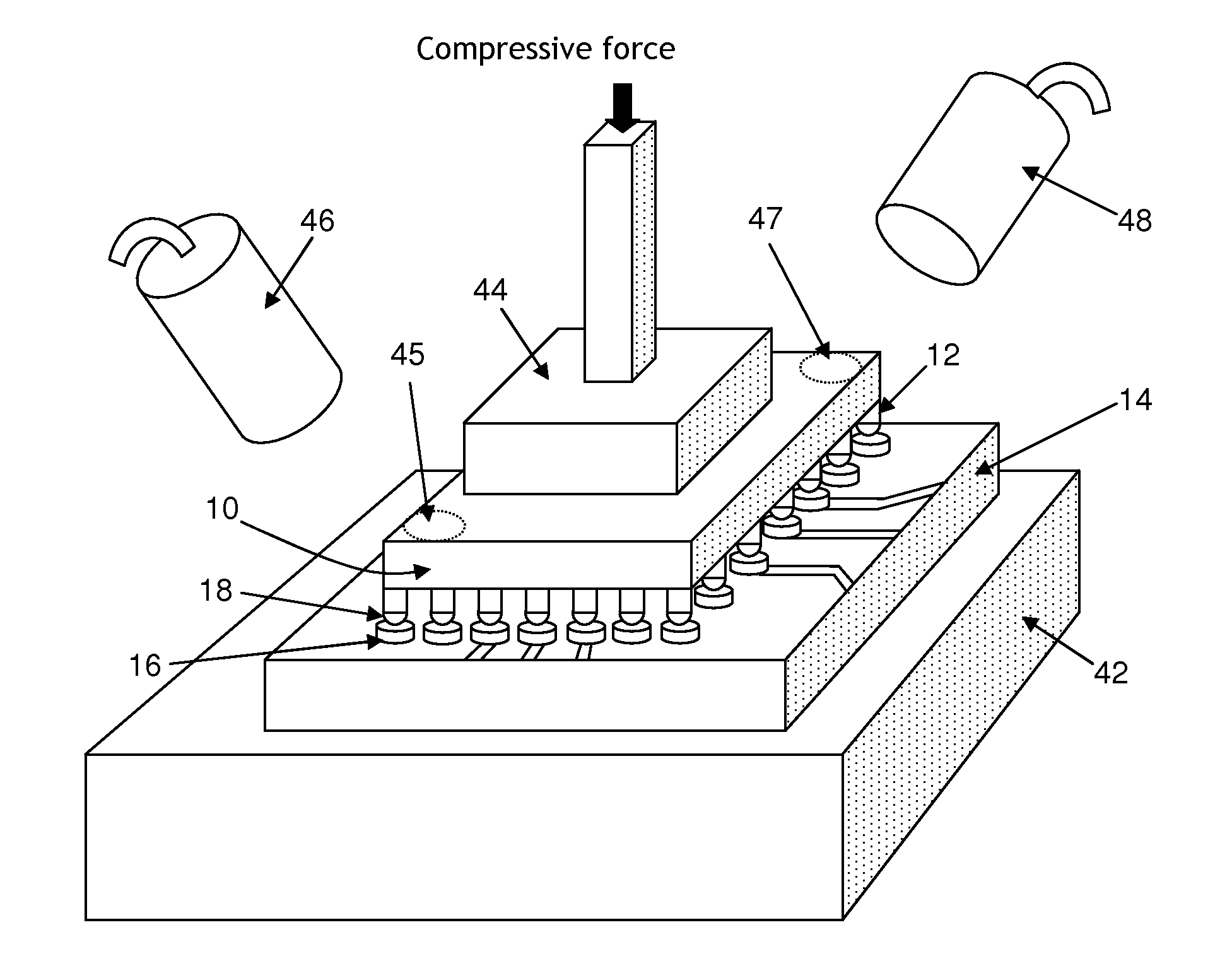
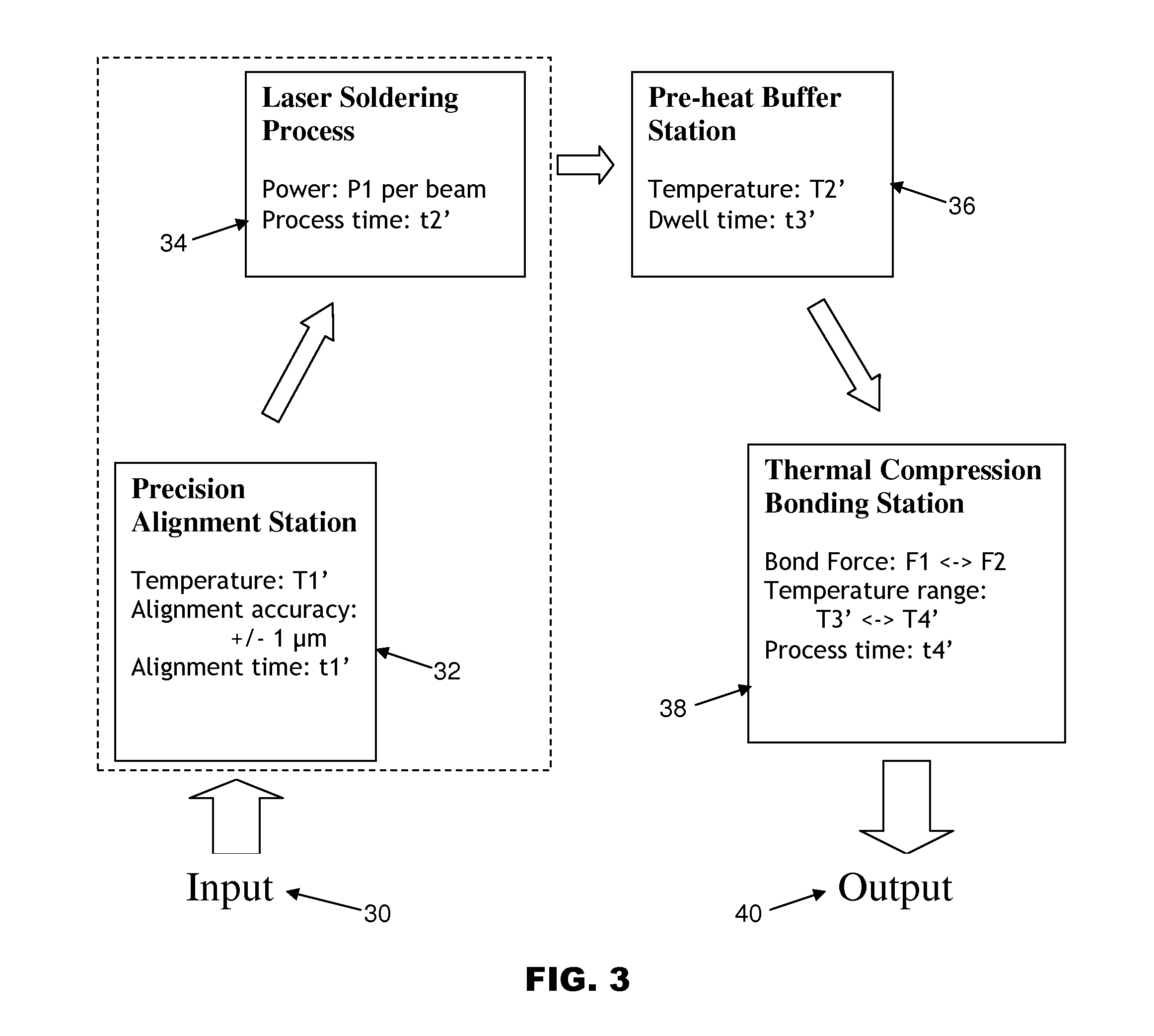
[0022]FIG. 3 is an overview of the bonding process according to the preferred embodiment of the present invention. The process enables parallel processing of the two major assembly processes, namely the precision alignment process and thermal compression bonding. The thermal compression bonder comprises the precision alignment station 32, the thermal compression bonding station 38 and a buffer station 36. The buffer station 36 is used as buffer for balancing the process flow as well as pre-heating the partially-bonded unit.

[0023]At the precision alignment station 32, both the precision alignment process and the laser soldering process 34 are carried out. All these process stations may reside in different parts of the thermal compression bonder, and a robotic arm may be used to transport the processing flip-chip from one processing station to another. The material flow of the system is described below.

[0024]The substrate 14 is loaded from an input port 30 by an input loader and the f...


PUM

PropertyMeasurementUnit
diameteraaaaaaaaaa
wavelengthaaaaaaaaaa
temperatureaaaaaaaaaa

Abstract

A die is prepared for thermal compression bonding by first aligning electrical contacts on the die to bond pads on a substrate onto which the die is to be mounted. Those electrical contacts are held against the bond pads on the substrate with a bonding tool. Partially bonding the die onto the substrate by providing heat to a portion of the die to elevate a temperature there to above a melting point of solder in the electrical contacts so as to melt at least some of the solder. Then thermally compress the whole die and heat it to above the melting point of the solder of the electrical contacts so that the solder of the electrical contacts outside the portion of the die are also melted to bond the die to the substrate.

Description

FIELD OF THE INVENTION[0001]The invention relates to the attachment of semiconductor chips onto substrates, particularly by way of solder interconnects.BACKGROUND AND PRIOR ART[0002]Solder reflow during the assembly of flip-chip packages is widely adopted in the electronic packaging industry. The interconnects of flip-chip silicon dies are commonly made of solder balls or bumps in area-array arrangement. The die is aligned and accurately placed onto a substrate such as a printed wiring board (“PWB”) so that the solder balls land on the solder pads of the substrate, from where the interconnects of the die are connected to the electrical circuit of the substrate. The solder pads comprise copper trace circuitry (with thickness of about 18 μm) coated with nickel (with thickness of about 6 μm) and gold (with thickness of less than 0.1 μm). An appropriate amount of solder flux will be applied to the soldering surfaces prior to the die placement process. Application of solder flux can prom...

Claims


Application Information

Patent Timeline
Patent Type & Authority Applications(United States)
IPC IPC(8): B23K26/00B23K3/04B23K31/02
CPCH01L24/13H01L24/16H01L24/75H01L24/81H01L2224/13082H01L2224/13111H01L2224/13147H01L2224/16238H01L2224/75251H01L2224/75744H01L2224/75753H01L2224/78252H01L2224/81121H01L2224/81191H01L2224/81203H01L2224/81224H01L2224/81986H01L2224/9205H01L2924/15192H01L2924/15311H01L2224/81048H01L2224/75263H01L2224/78253H01L2924/07802H01L2224/81907H01L2924/12042H01L2924/00014H01L2924/014H01L2924/01047H01L2924/01029H01L2924/00
Inventor CHEUNG, YIU MINGLO, TSAN YIN PETERLI, MINGMAK, YICK HONGLAM, KA SAN
Owner ASMPT SINGAPORE PTE LTD
Why Eureka
Try Eureka