
Amorphous phase yttrium-doped indium zinc oxide thin film transistors and method for making same

a thin film transistor and yttrium-doped indium zinc oxide technology, applied in the field of thin film transistors and method for making same, can solve the problems of suppressing carrier concentration, affecting the doping ratio of elements, so as to achieve accurate doping ratio and reduce cost

Inactive Publication Date: 2014-01-16
NATIONAL CHUNG CHENG UNIV
View PDF3 Cites 6 Cited by
  • Summary
  • Abstract
  • Description
  • Claims
  • Application Information

AI Technical Summary

Benefits of technology

The present invention is a non-vacuum solution process for fabricating TAOS. This technology aims to create accurate doping ratios and reduce costs. The invention uses a new TAOS material with a molarity ratio of indium to zinc of 1:1. The process uses yttrium as the dopant in the IZO system to suppress carrier concentration and create yttrium-doped indium zinc oxide thin film transistors (YIZO TFTs). The invention also explores the electronegativity and standard electrode potentials of the elements, which help in the formation of strong bonds and the suppression of oxygen vacancies. Overall, the invention provides a cost-effective and accurate way to create high-quality TFTs.

Problems solved by technology

However, as the drain voltage increases and exceeds the gate voltage, the inversion layer charge that is near the drain becomes zero, and thus the channel disappears, which is called pinch-off.
The result of this publication showed that lower defect density results in steep subthreshold swing.
However, according to the prior arts mentioned above, many problems remain unsolved: effectively suppressing carrier concentration, shift of VT toward positive voltage, lowering off current, increasing optical band gap (Eopt) and improving visible light transmission.

Method used


Image

  • Amorphous phase yttrium-doped indium zinc oxide thin film transistors and method for making same
  • Amorphous phase yttrium-doped indium zinc oxide thin film transistors and method for making same
  • Amorphous phase yttrium-doped indium zinc oxide thin film transistors and method for making same

Examples


first embodiment

[0082]This is an embodiment illustrative of the equipments, instruments, materials and methods of use involved in the embodiments of the present invention.

[0083]1. Processing Equipment: Spin Coater

[0084]The spin coater was from Professor Chu-Chi Ting's lab at National Chung Cheng University and the spin coater was placed in a class-100 clean glovebox. A clean syringe and a 0.20 um syringe filter were used to drop precursor on a substrate. The spin coating process is divided into two stages with two different spin-coating rate. During the first stage, solution was coated on the substrate evenly. During the second stage, the coating thickness of the coating layer was then controlled.

[0085]2. Processing Equipment: Tube Furnace

[0086]The tube furnace for sintering in the illustrative embodiments of the present invention was from Professor Chu-Chi Ting's lab at National Chung Cheng University that was purchased from Chitun Industry Corporation in Changhua County. The organic carbon chain ...

second embodiment

[0135]The present embodiment relates to the cleaning procedure of the silicon substrates.

[0136]To ensure the quality of the coating, the substrates must be cleaned before coating in order to remove organic-matter and dust. The cleaning procedure of the substrates comprised sequential steps as follows:

[0137]1. A substrate was put in a crystallizing basin containing diluted detergents (diluted with deionized water), and then the crystallizing basin was put into a sonicator to sonicate for 10 minutes in order to remove the oil on the substrate surface. The substrate was washed with deionized water, and then the substrate was dried.

[0138]2. The substrate was put in a crystallizing basin containing acetone, and then the crystallizing basin was put into a sonicator to sonicate for 10 minutes in order to remove the organic-matter on the substrate surface.

[0139]3. The substrate was removed from acetone and was put in a crystallizing basin containing IPA, and then the crystallizing basin was...

third embodiment

[0142]The present embodiment relates to the procedure of preparing solution for coating the active layer.

[0143]The molarity of indium and zinc of the active layer used in the present invention was 0.224 M. The ratios of doping amount of yttrium to the molarity of indium were different wherein the doping amounts of yttrium were 0, 2, 4, 6, 8, 12, 14, 20% respectively. The procedure of preparing solution for coating the active layer was as follows:

[0144]1. Zinc (II) nitrate hydrate was added into 2′-O-(2-methoxy) ethyl (2-MOE) and zinc (II) nitrate hydrate was dissolved. The dissolving rate of the solute was increased by sonication for 10 minutes to get a solution.

[0145]2. Indium (III) nitrate hydrate was added into the solution and indium (III) nitrate hydrate was dissolved. The dissolving rate of the solute was increased by sonication for 10 minutes to get the solution.

[0146]3. Yttrium (III) nitrate hydrate was added into the solution and yttrium (III) nitrate hydrate was dissolved....


PUM


Abstract

Sol-gel-processed thin-film transistors (TFTs) with amorphours Y—In—Zn—O (YIZO) as an active layer are fabricated with various mole ratios of Y, which indicates that Y3+ could play the role of carrier suppressor in InZnO (IZO) systems and reduce off current of YIZO-TFT and its channel mobility, threshold voltage, subthreshold swing voltage, and on / off ratio.

Description

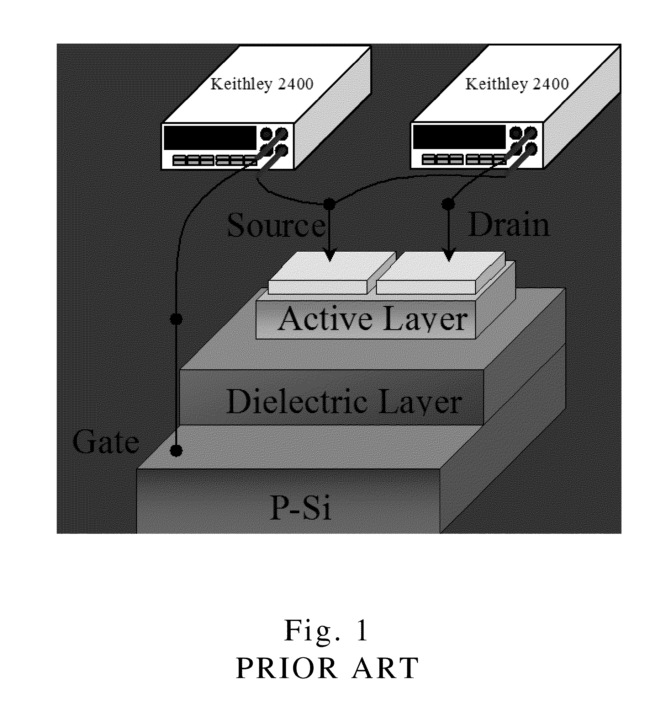
BACKGROUND OF THE INVENTION[0001]1. Field of the Invention[0002]The present invention relates to thin film transistors and method for making same, and particularly to amorphous phase yttrium-doped indium zinc oxide thin film transistors and method for making same.[0003]2. Description of Related Art[0004]The working principle and properties of the thin film transistor (TFT) are related to the structures and the device operation of the TFT. According to the structure, the TFT can be classified into top gate and bottom gate based on the position of the gate electrode while it also can be classified into top contact and bottom contact based on the position of source electrode and drain electrode, and thus the TFT has four different structures, as shown in Rolland, A. et al. J. Electrochem. Soc. 140, 3679-3683 (1993). The channel length (L) and the channel width (W) of the channel of the active layer that is between the source and the drain are important parameters.[0005]As mentioned in ...

Claims


Application Information

Patent Timeline
Patent Type & Authority Applications(United States)
IPC IPC(8): H01L29/24H01L29/786H01L21/336H01L21/36
CPCH01L21/02554H01L21/02565H01L21/02581H01L29/247H01L29/78693
Inventor TING, CHU-CHICHANG, HSIEH-PING
Owner NATIONAL CHUNG CHENG UNIV
Learn More