Manufacturing method for a semiconductor on insulator type substrate for radiofrequency applications

a technology of insulator and substrate, which is applied in the direction of semiconductor devices, basic electric elements, electrical apparatus, etc., can solve the problems of poor logical device characteristics, low resistivity layer, and poor radiofrequency performance of soq and sos substrates

Active Publication Date: 2014-03-27
COMMISSARIAT A LENERGIE ATOMIQUE ET AUX ENERGIES ALTERNATIVES +1
View PDF5 Cites 126 Cited by
  • Summary
  • Abstract
  • Description
  • Claims
  • Application Information

AI Technical Summary

Problems solved by technology

These substrates give excellent radiofrequency performances but have very poor characteristics concerning logical devices, due to the lower quality of the silicon.
They are also very expensive.
Such substrates are particularly advantageous for the functioning of logical devices, but their radiofrequency performances are not as good as SOQ and SOS substrates.
These substrates have the disadvantage that they sometimes include a low resistivity layer under the oxide layer.
The presence of this low resistivity layer may be due to surface contamination of the substrates (for example due to condensation of boron and/or phosphorus) before bonding.
However, oxygen atoms can diffuse in the substrate before or during this treatment, which leads to the formation of regions in the substrate with a low precipitation rate—and therefore low resistivity —, particularly close to the surface of the substrate.
These two causes are difficult to control at the moment.
Different techniques have been developed for this purpose but they have the disadvantage that they are very sensitive to heat treatments used to manufacture the SOI and then devices on the SOI.
However, the polycrystalline silicon recrystallises at high temperature, and doping agents present at the interface between the polycrystalline silicon layer and the HR silicon substrate diffuse in the HR silicon substrate, which has the effect o

Method used


Image

  • Manufacturing method for a semiconductor on insulator type substrate for radiofrequency applications
  • Manufacturing method for a semiconductor on insulator type substrate for radiofrequency applications
  • Manufacturing method for a semiconductor on insulator type substrate for radiofrequency applications

Examples


example embodiment

of the Invention

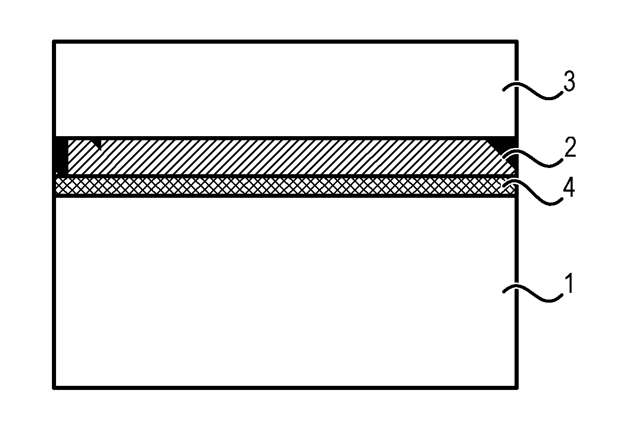
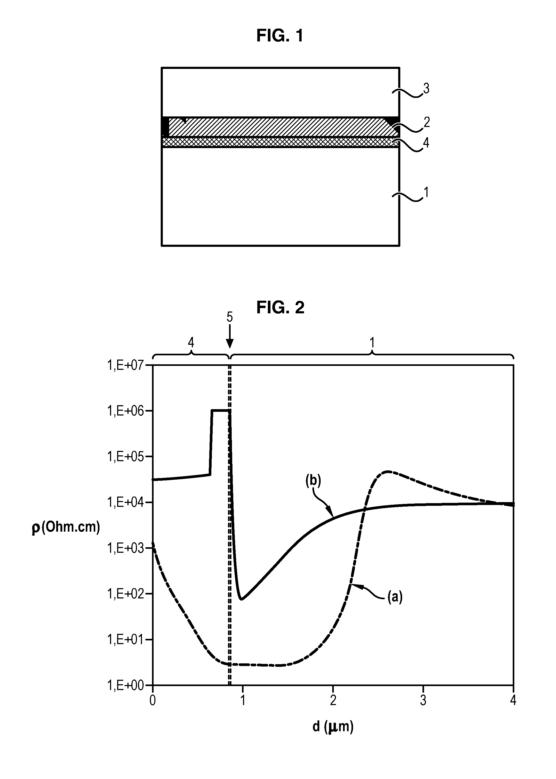
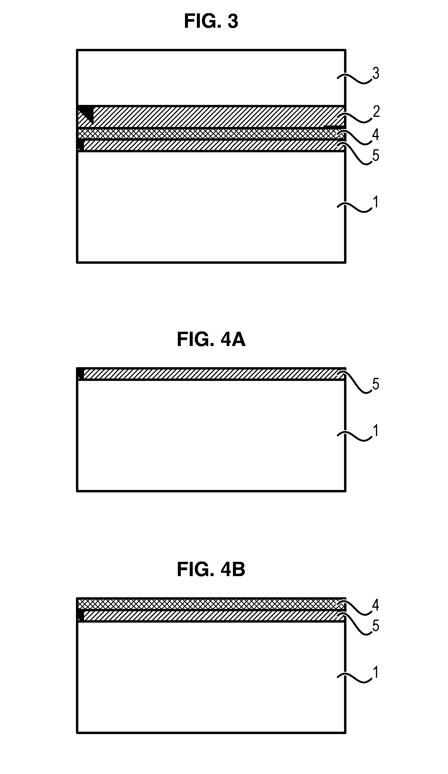
[0147]A first step consists of applying special cleaning of the high resistivity silicon substrate.

[0148]The purpose of this cleaning is to minimise the quantity of doping agents (mainly boron and phosphorus atoms) at the substrate surface.

[0149]An appropriate cleaning method may for example include cleaning with hydrofluoric acid (HF) diluted to 0.2% to remove the chemical oxide, followed successively by cleaning with ozone and then hydrochloric acid (HCl) to form a thin layer of oxide (in other words with a thickness of about 0.7 to 0.8 nm). This cycle can be repeated twice to increase consumption of the silicon surface on which undesirable contaminants are located.

[0150]The next step is to form a thin layer of oxide (about 0.5 to 10 nm) on the surface of the high resistivity silicon substrate.

[0151]Adapted techniques include a standard thermal oxidation treatment known to those skilled in the art as Rapid Thermal Oxidation (RTO), dry thermal oxidation or a low te...


PUM


Abstract

The invention relates to a method for manufacturing a semiconductor on insulator type substrate for radiofrequency applications, comprising the following steps in sequence: (a) provision of a silicon substrate (1) with an electrical resistivity of more than 500 Ohm·cm, (b) formation of a polycrystalline silicon layer (4) on said substrate (1), said method comprising a step between steps a) and b) to form a dielectric material layer (5), different from a native oxide layer, on the substrate (1), between 0.5 and 10 nm thick.

Description

DOMAIN OF THE INVENTION[0001]This invention relates to a method for manufacturing a semiconductor on insulator type substrate for radiofrequency applications and a substrate obtained using said method.BACKGROUND OF THE INVENTION[0002]There are different types of substrates for making radiofrequency (RF) devices at the present time.[0003]A first type of substrate includes substrates comprising a silicon layer on an insulating substrate, for example such as Silicon on Quartz (SOQ), Silicon on Sapphire (SOS) or Silicon on Glass (SOG) substrates.[0004]These substrates give excellent radiofrequency performances but have very poor characteristics concerning logical devices, due to the lower quality of the silicon. They are also very expensive.[0005]A second type of substrate is a High Resistivity (HR) bulk Silicon substrate. High Resistivity Means Especially an Electrical Resistivity of More than 500 Ohm·cm.[0006]Performances of these substrates are lower than the performances of the fir...

Claims


Application Information

Patent Timeline
IPC IPC(8): H01L21/02H01L29/06H01L29/04
CPCH01L21/02381H01L29/06H01L29/04H01L21/76254H01L21/02052H01L21/32155H01L21/324
Inventor ALLIBERT, FREDERICWIDIEZ, JULIE
Owner COMMISSARIAT A LENERGIE ATOMIQUE ET AUX ENERGIES ALTERNATIVES
Why Eureka
Try Eureka