Films of Nitrides of Group 13 Elements and Layered Body Including the Same

a technology of nitride and layered body, which is applied in the direction of crystal growth process, polycrystalline material growth, chemistry apparatus and processes, etc., can solve the problem of the viewpoint limit, and achieve the effect of reducing the crystal dislocation and preferable properties

Active Publication Date: 2014-07-17
NGK INSULATORS LTD
View PDF2 Cites 8 Cited by
  • Summary
  • Abstract
  • Description
  • Claims
  • Application Information

AI Technical Summary

Benefits of technology

[0016]That is, by growing a nitride single crystal including inclusions with a size of several microns or so only in a region having a thickness of 50 microns during an initial stage of the crystal growth by flux method, it is possible to considerably reduce the dislocation of the crystal and thereby to provide preferable properties for various devices. Such discovery is made contrary to common knowledge of skilled artisans in the art of growing nitride single crystals by flux method.

Problems solved by technology

However, there has been a technical limit on this viewpoint and the breakthrough has thus been demanded.

Method used


Image

  • Films of Nitrides of Group 13 Elements and Layered Body Including the Same
  • Films of Nitrides of Group 13 Elements and Layered Body Including the Same
  • Films of Nitrides of Group 13 Elements and Layered Body Including the Same

Examples


##ventive example 1

Inventive Example 1

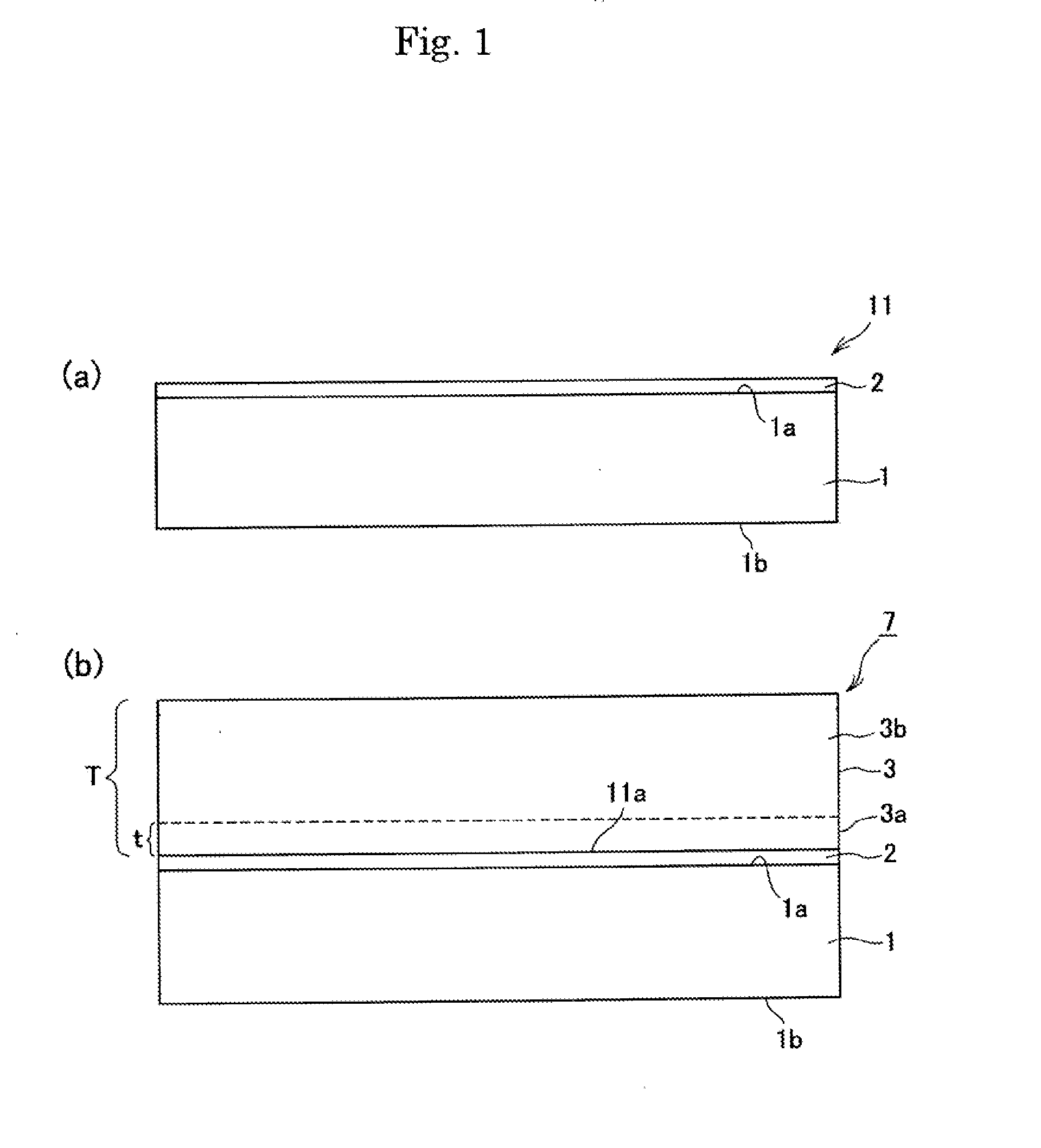
[0080]The crystal production system shown in FIGS. 4 and 5 was used to produce gallium nitride crystal. The procedure will be described below. First, in a glove box filled with argon atmosphere, it is provided a seed crystal substrate (GaN template of φ 2 inches: GaN thin film (thickness of 5 microns) is formed on a sapphire substrate by MOCVD process) horizontally on a bottom of the crucible 14 having an inner diameter φ of 70 mm.

[0081]At this stage, the defect density at the surface of the GaN thin film was evaluated by CL (Cathode Luminescence) and proved to be about 8×10⁸ to 2×10⁹ / cm2.

[0082]Then, 15 g of sodium metal, 10 g of gallium metal and 39 mg of carbon (Ga / Na ratio was 18 mol %, C / Na ratio was 0.5 mol %) were charged into the crucible 14. The crucible 14 was contained in the inner container 16 made of stainless steel, and the inner container 16 was then contained in the outer container 14. An opening of the outer container main body was closed with the ...

##ventive example 2

Inventive Example 2

[0087]The gallium nitride film was formed according to the same procedure as the Inventive Example 1. However, the rotational direction was periodically inverted. Further, the acceleration time period was 1 second, retention time period was 15 seconds, deceleration time period was 1 second, and stopping time period was 3000 seconds, and the inversion of the rotational direction was repeated.

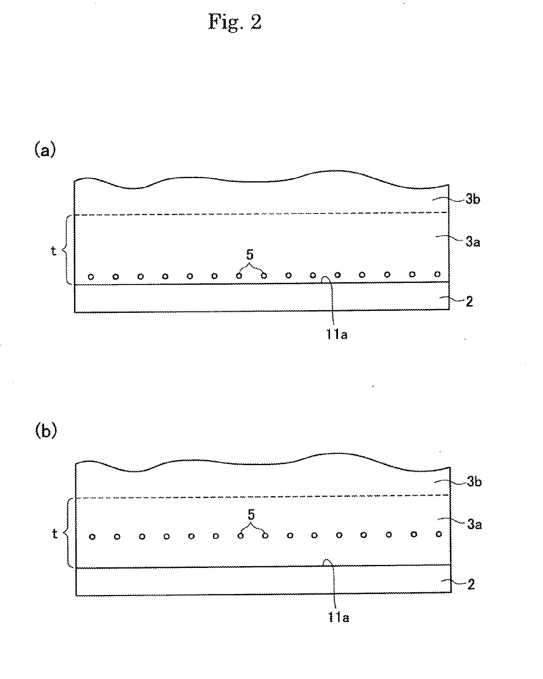
[0088]The cross section of the thus grown crystal was observed and the results were shown in FIG. 7. FIG. 15 shows the binarized image thereof. As can be seen form the figures, it was proved that inclusions each having a size of several microns were present in a region distant from the interface by 40 μm or smaller in the initial stage of growth. The inclusions were subjected to SIMS analysis to detect sodium and gallium. Further, the ratio of the area of the inclusions in each layer was shown in table 1. Besides, the ratio of the area of the inclusions in the region distant fr...

##ventive example 3

Inventive Example 3

[0090]The gallium nitride film was formed according to the same procedure as the Inventive Example 1. However, the rotational direction was periodically inverted. Further, the acceleration time period was 1 second, retention time period was 15 seconds, deceleration time period was 1 second, and stopping time period was 3000 seconds, and the inversion of the rotational direction was repeated. The rotation speed was made 10 rpm.

[0091]The cross section of the thus grown crystal was observed and the results were shown in FIG. 8. FIG. 16 shows the binarized image thereof. As can be seen form the figures, it was proved that inclusions each having a size of several microns were present in a region distant from the interface by 50 μm or smaller in the initial stage of growth. The inclusions were subjected to SIMS analysis to detect sodium and gallium. Further, the ratio of the inclusions in each layer was shown in table 1. Besides, the ratio of the area of the inclusions ...


PUM

PropertyMeasurementUnit
areaaaaaaaaaaa
thicknessaaaaaaaaaa
thicknessaaaaaaaaaa

Abstract

A film 3 of a nitride of a group 13 element is grown on a seed crystal substrate 11 by flux process from a melt containing a flux and a group 13 element under nitrogen containing atmosphere. The film 3 of a nitride of a group 13 element includes an inclusion distributed layer 3a in a region distant from an interface of the film of a nitride of group 13 element on the side of the seed crystal substrate 11 and containing inclusions derived from components of the melt, and an inclusion depleted layer 3b, with the inclusion depleted. provided on the layer 3a.

Description

FIELD OF THE INVENTION[0001]The present invention relates to a film of nitride of group 13 element and a layered body including the same. The film of nitride of group 13 element and layered body can be used for a white LED with improved color rendering index, a blue-violet laser disk for high-speed and high-density optical memory, a power device for an inverter for a hybrid car or the like.BACKGROUND ARTS[0002]It has been recently and intensively studied that a nitride of a group 13 element such as gallium nitride is used to produce a semiconductor device such as a blue ray laser, white ray laser, blue-violet ray semiconductor laser and the like and that the device is applied to various kinds of electronic appliances.[0003]Such prior gallium nitride-based semiconductor device has been mainly produced by vapor phase process. Specifically, it has been produced by growing a thin film of gallium nitride by heteroepitaxial growth on a sapphire or silicon carbide substrate by organic meta...

Claims


Application Information

Patent Timeline
Patent Type & Authority Applications(United States)
IPC IPC(8): H01L33/32
CPCH01L33/32C30B19/02C30B29/403H01L21/0237H01L21/0242H01L21/02458H01L21/0254H01L21/02576H01L21/02625H01L33/007C30B29/38H01L21/208
Inventor IWAI, MAKOTOHIRAO, TAKAYUKIYOSHINO, TAKASHI
Owner NGK INSULATORS LTD
Why Eureka
Try Eureka