

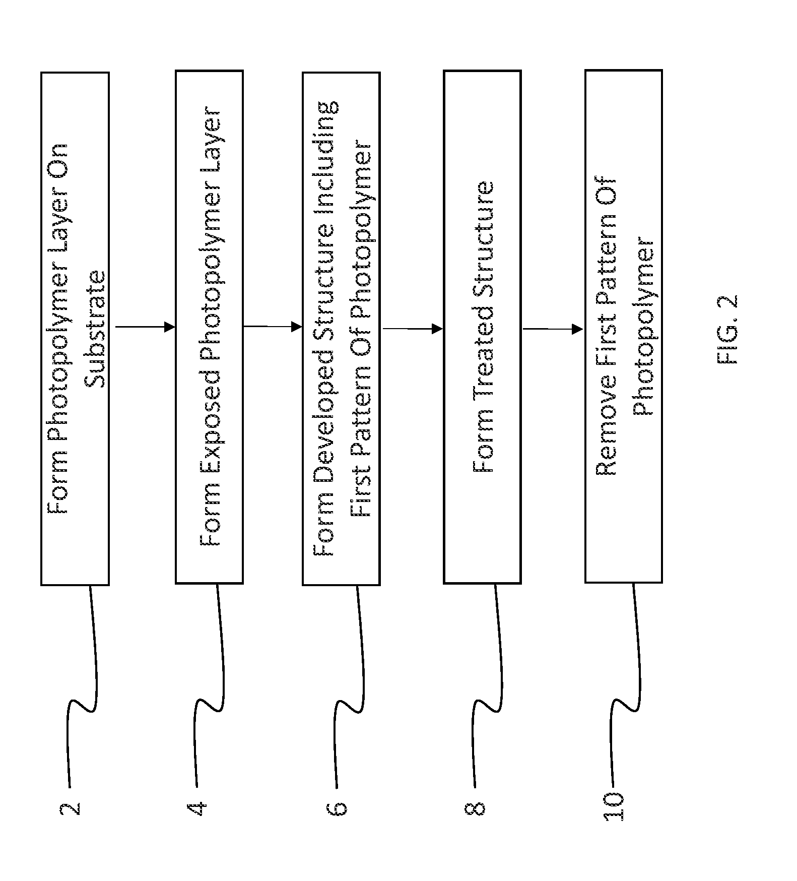
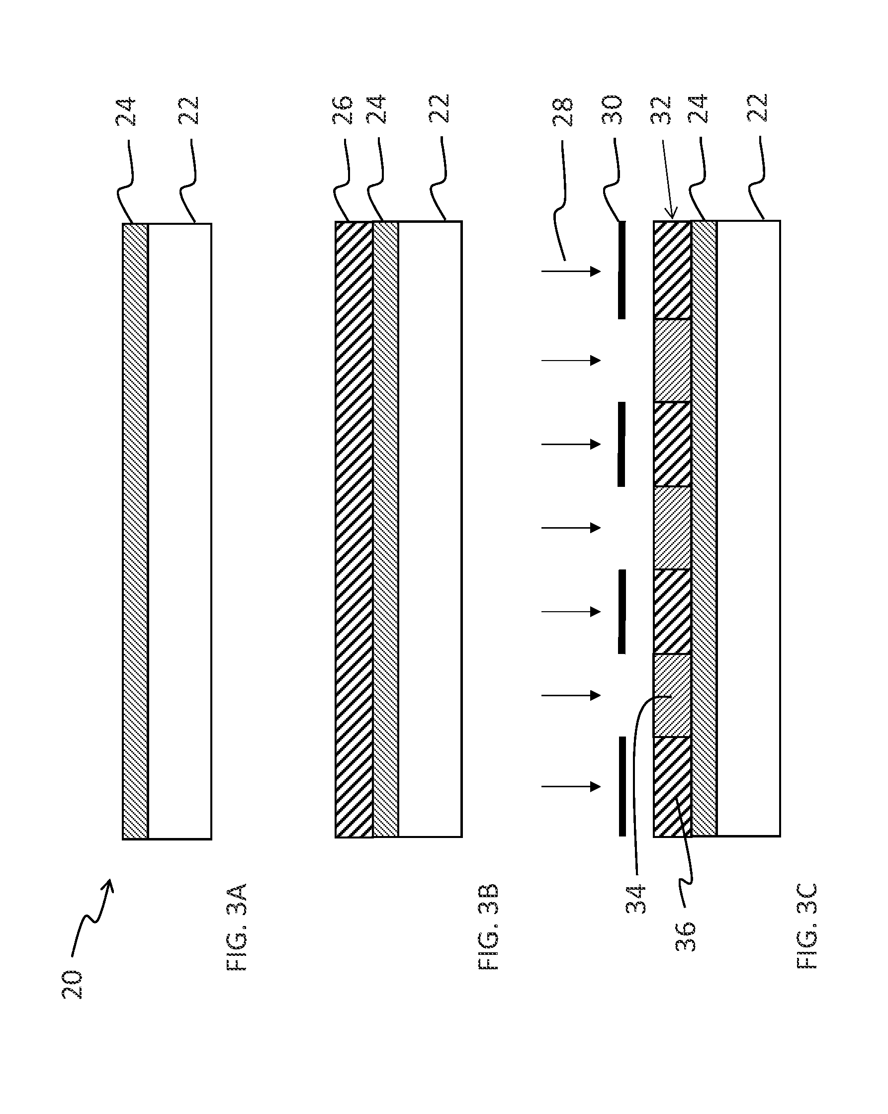
Method of patterning a device
a technology of switchable photopolymer and patterning device, which is applied in the field of acidcatalyzed switchable photopolymer, can solve the problems of reducing the resistance of organic materials to solvents, affecting the development of devices based on these materials, and affecting the quality of organic electronics, etc., so as to reduce the use of fluorinated functional groups, reduce the fluorine content of photopolymers, and reduce the manufacturing cost
- Summary
- Abstract
- Description
- Claims
- Application Information
AI Technical Summary
Benefits of technology
Problems solved by technology
Method used
Image

Examples
synthesis example 1 (
Poly-TBMA)
[0073]To a 250 mL jacketed four-necked flask equipped with a teflon-blade stirrer, a reflux condenser with a mineral oil bubbler outlet, sub-surface nitrogen sparge tube, and a thermometer was charged 28.4 g (˜32.5 m L, 0.2 mol.) tert-butyl methacrylate (TBMA), 87.2 g (˜56.5 mL) HFE-7600 and 0.723 g (4.38 mmol.) AIBN [2.5 wt % initiator level]. The agitator motor was programmed for 200 rpm stirring. The sparge tube was adjusted so it is below the surface of the solution and nitrogen was bubbled subsurface for 1 hour. During the sparge, the constant temperature bath (CTB) connected to the jacket of the reaction flask was preheated to 76° C. with flow to the flask turned off. When the nitrogen sparge was complete the nitrogen flow was reduced so that a slight positive flow was maintained throughout the reaction. The valves to the CTB were opened to the reaction flask. The reaction was stirred for 20 hours at 200 rpm with 76° C. fluid circulating through the flask jacket. The...
example 1
[0076]A composition comprising 8% by weight solution of poly-TBMA in HFE-7600 from Synthesis Example 1 (0% fluorine by weight) was spin coated onto a Si wafer at 1000 rpm to form a photopolymer layer approximately 1.5 μm thick. The film was post apply baked on a hot plate at 90° C. for 60 seconds to remove excess solvent. The bake temperature or time can be adjusted to control the free volume of the polymer film to control such aspects as PAG diffusion or airborne amine penetration that can cause “amine poisoning” of the surface, causing less acid reaction near the surface compared with the bulk of the film. Temperature may also be lowered to work with a particularly temperature sensitive active organic material that may be underneath the photopolymer layer or with a temperature sensitive support, such as PET. An oven bake may also be used instead of the hot plate bake.
[0077]The photopolymer layer was exposed to UV radiation, activating the photo-acid through light absorption by the...
example 2
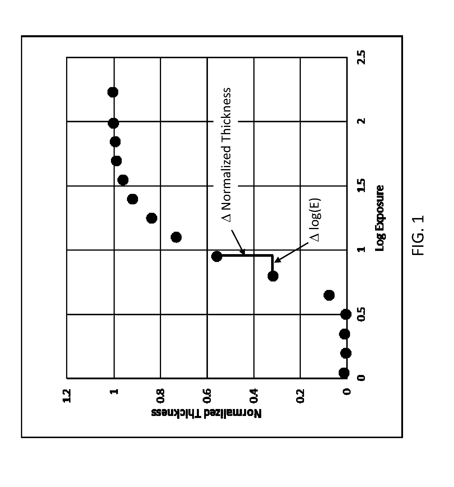
Dissolution Rate Measurements
[0080]A series of photopolymer solutions were prepared using HFE-7600 as coating solvent, CGI 1907 as PAG (2.0% by wt relative to polymer wt), and photopolymers prepared by copolymerizing TBMA with various amounts of FOMA, the mol ratios for which are shown in Table 1. The dissolution rate for unexposed polymers coated on Si wafers were measured by interferometry using a Filmetrics F20 Thin-Film Analyzer using either HFE-7600 or HFE-6512 as the hydrofluoroether developing solvent. The dissolution was usually directly proportional to contact time indicating that mass transport was not rate-limiting.
TABLE 1TBMA / FOMADissolution rate (nm / sec)typemol ratio (%)% F by weightHFE-6512HFE-7600Comp 50 / 5042.8>1000770Inv93 / 710.65018Inv95 / 57.93913Inv97 / 34.93512Inv99 / 11.75219Inv100 / 0 04615
[0081]The solubility of copolymers of TBMA at low FOMA levels was surprising. One can see a downward trend in dissolution rates as FOMA level gets lower, but the dissolution rates are...
PUM
 Abstract
Description
Claims
Application Information