Semiconductor device

a semiconductor device and semiconductor technology, applied in the direction of transistors, electroluminescent light sources, electric lighting sources, etc., can solve the problems of increasing the increase of the electrical characteristics, the increase of the transistor over time or due to a stress test, etc., to achieve the effect of increasing the aperture ratio in a pixel, reducing the number of steps of manufacturing the semiconductor device, and increasing the area occupied by the capacitor

Active Publication Date: 2014-11-20
SEMICON ENERGY LAB CO LTD
View PDF3 Cites 48 Cited by
  • Summary
  • Abstract
  • Description
  • Claims
  • Application Information

AI Technical Summary

Benefits of technology

[0021]On an element substrate of one embodiment of the present invention, one electrode of the capacitor is formed at the same time as the oxide semiconductor film of the transistor. In addition, the conductive film that serves as a pixel electrode is used as the other electrode of the capacitor. Thus, a step of forming another conductive film is not needed to form the capacitor, and the number of steps of manufacturing the semiconductor device can be reduced. Further, since the pair of electrodes has a

Problems solved by technology

The transistor having normally-on characteristics causes various problems in that malfunction is likely to be caused when in operation and that power consumption is increased when not in operation,

Method used


Image

  • Semiconductor device
  • Semiconductor device
  • Semiconductor device

Examples


embodiment 1

[0052]In this embodiment, a semiconductor device that is one embodiment of the present invention is described with reference to drawings. Note that in this embodiment, a semiconductor device of one embodiment of the present invention is described taking a display device as an example. In addition, an oxide semiconductor film is used as a semiconductor film in this embodiment.

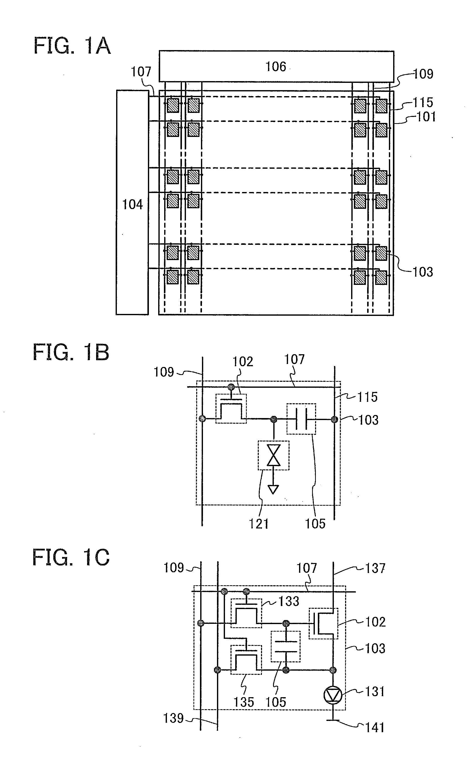
[0053]FIG. 1A illustrates an example of a semiconductor device. The semiconductor device in FIG. 1A includes a pixel portion 101, a scan line driver circuit 104, a signal line driver circuit 106, m scan lines 107 which are arranged in parallel or substantially in parallel and whose potentials are controlled by the scan line driver circuit 104, and n signal lines 109 which are arranged in parallel or substantially in parallel and whose potentials are controlled by the signal line driver circuit 106. Furthermore, the pixel portion 101 includes a plurality of pixels 103 arranged in a matrix. In addition, capacitor ...

embodiment 2

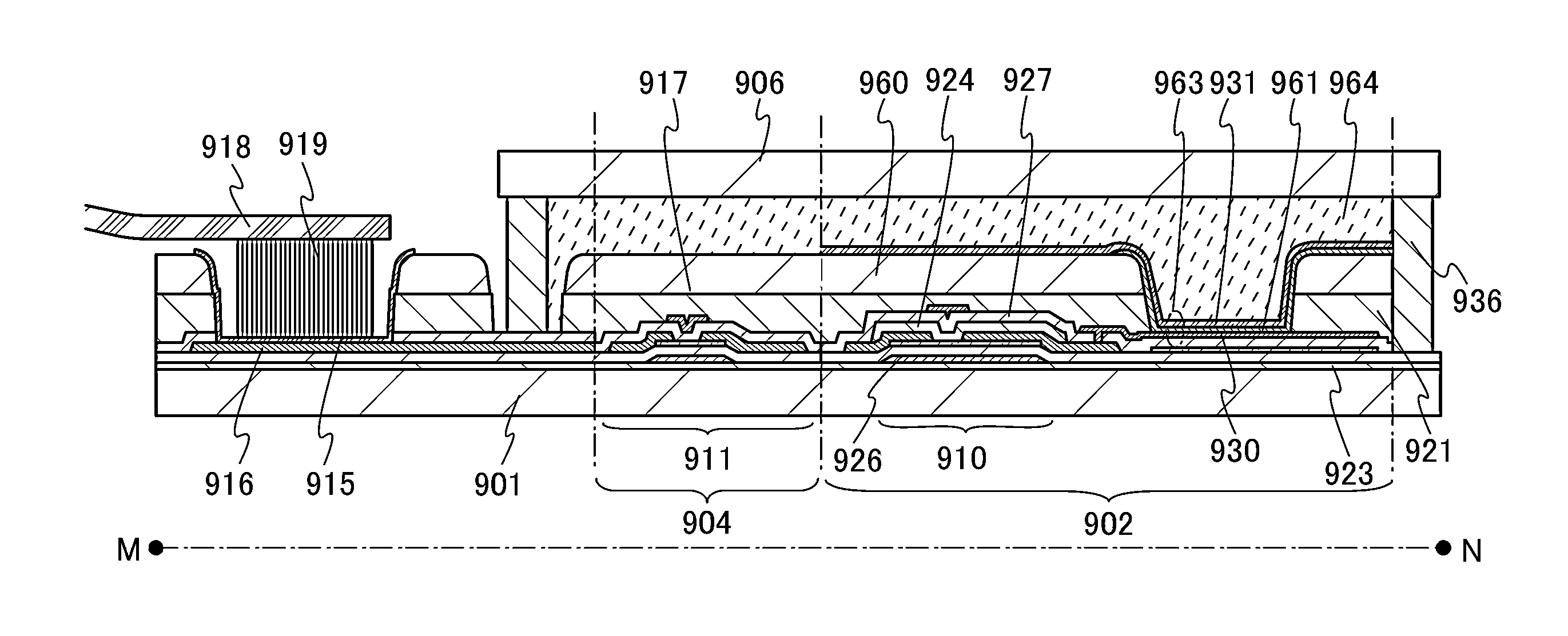
[0216]In this embodiment, a semiconductor device and a manufacturing method thereof, which are different from those shown in Embodiment 1, are described with reference to the drawings. The semiconductor device in this embodiment is different from that in Embodiment 1 in that the transistor has a structure in which an oxide semiconductor film is provided between different gate electrodes, that is, a dual-gate structure. Note that the description about the same structures as those in Embodiment 1 is omitted.

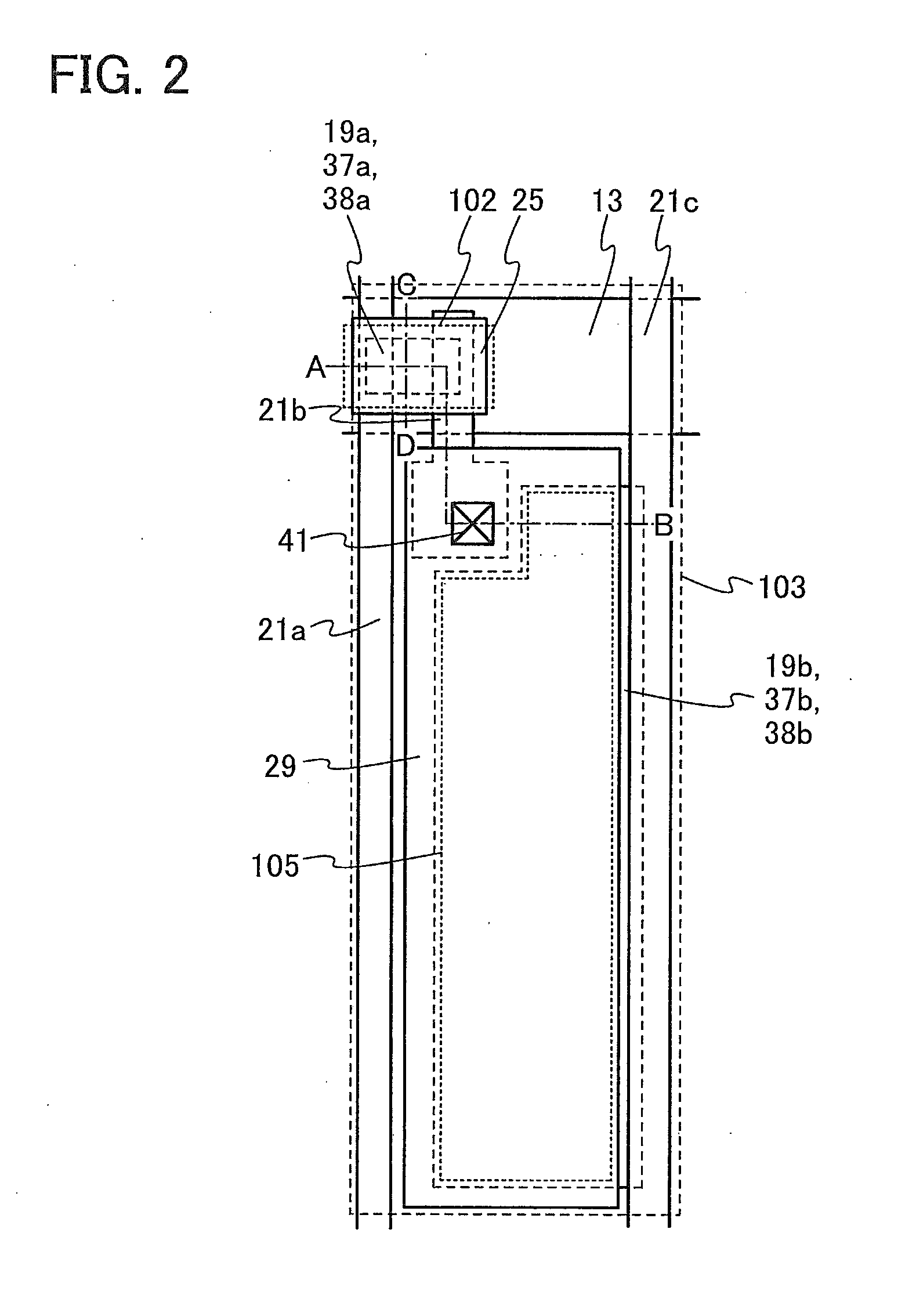
[0217]A specific structure of an element substrate included in the display device is described. Here, a specific example of a liquid crystal display device including a liquid crystal element in the pixel 103 is described. FIG. 8 is a top view of the pixel 103 illustrated in FIG. 1B.

[0218]The structure in this embodiment is different from that in Embodiment 1 in that, in a plan view of the pixel 103 in FIG. 8, a conductive film 29a serving as a gate electrode and overlapping part of...

embodiment 3

[0246]In this embodiment, the electrical characteristics of the transistor having a dual-gate structure described in Embodiment 2 that includes gate electrodes connected to each other and having the same potential are described with reference to FIG. 9 and FIGS. 11A to 16C.

[0247]Note that here a driving method in which the conductive films 13 and 29a serving as gate electrodes in FIG. 9 are electrically short-circuited and are supplied with a gate voltage is referred to as dual-gate driving. In other words, in dual-gate driving, the voltages of the conductive films 13 and 29a serving as gate electrodes are always equal to each other.

[0248]Here, the electrical characteristics of the transistor were evaluated. FIGS. 11A and 11B illustrate the structures of transistors used for the calculation. Note that device simulation software “Atlas” produced by Silvaco Inc. was used for the calculation.

[0249]A transistor having Structure 1 in FIG. 11A is a dual-gate transistor.

[0250]In the transi...


PUM


Abstract

A semiconductor device including a transistor having excellent electrical characteristics is provided. Alternatively, a semiconductor device having a high aperture ratio and including a capacitor capable of increasing capacitance is provided. The semiconductor device includes a gate electrode, an oxide semiconductor film overlapping the gate electrode, an oxide insulating film in contact with the oxide semiconductor film, a first oxygen barrier film between the gate electrode and the oxide semiconductor film, and a second oxygen barrier film in contact with the first oxygen barrier film. The oxide semiconductor film and the oxide insulating film are provided on an inner side of the first oxygen barrier film and the second oxygen barrier film.

Description

BACKGROUND OF THE INVENTION[0001]1. Field of the Invention[0002]The present invention relates to a semiconductor device provided with a transistor including an oxide semiconductor film and a manufacturing method thereof.[0003]2. Description of the Related Art[0004]Attention has been focused on a technique for forming a transistor using a semiconductor thin film formed over a substrate (also referred to as thin film transistor (TFT)). Such a transistor is applied to a wide range of electronic devices such as an integrated circuit (IC) and an image display device (display device). A silicon-based semiconductor material is widely known as a material for a semiconductor thin film applicable to a transistor. As another material, an oxide semiconductor has been attracting attention.[0005]For example, a transistor including an oxide semiconductor containing indium (In), gallium (Ga), and zinc (Zn) as an active layer is disclosed (see Patent Document 1).[0006]Moreover, a technique in which ...

Claims


Application Information

Patent Timeline
IPC IPC(8): H01L29/786H05B44/00
CPCH01L29/7869H01L29/78606H01L29/4908H01L27/1225H01L27/1255H10K59/1216H10K59/1213
Inventor YAMAZAKI, SHUNPEIMIYAKE, HIROYUKIOKAZAKI, KENICHIHAYAKAWA, MASAHIKOMATSUDA, SHINPEI
Owner SEMICON ENERGY LAB CO LTD
Why Eureka
Try Eureka