

High brightness solid state illumination system for fluorescence imaging and analysis
- Summary
- Abstract
- Description
- Claims
- Application Information
AI Technical Summary
Benefits of technology
Problems solved by technology
Method used
Image

Examples
first embodiment
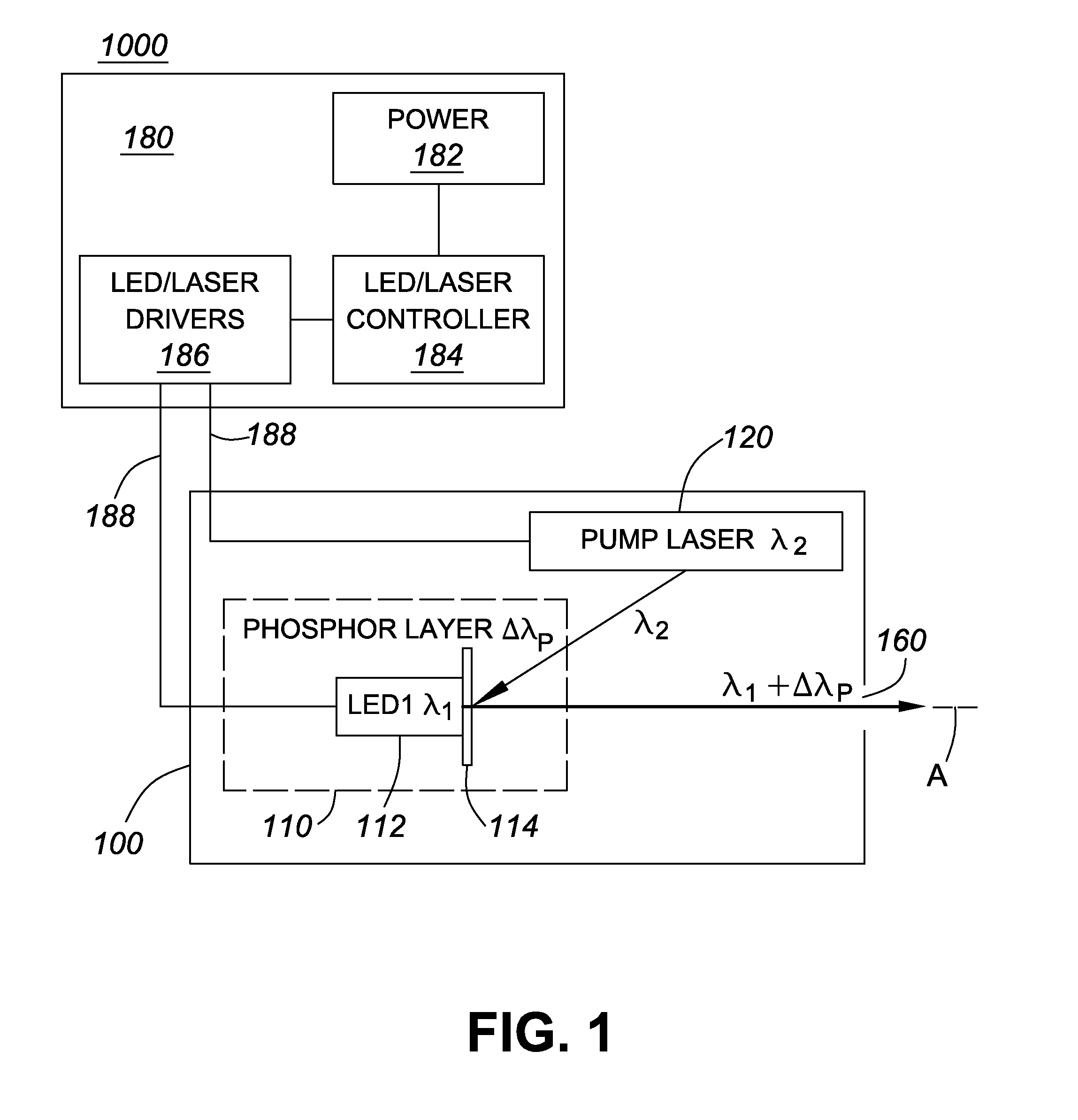
[0058]A schematic diagram showing elements of an illumination system 1000, according to the invention, is shown in FIG. 1. The illumination system 1000 comprises a light source unit or module 100 for providing high brightness illumination for fluorescence illumination and analysis. The light source unit 100 comprises first and second light sources 110 and 120. The first light source 110 comprises an LED 112 (LED1) and a phosphor layer 114, the LED 112 emitting a first wavelength λ1 within an absorption band of the phosphor layer and the phosphor layer 114 emitting broadband light emission of longer wavelength, comprising light in a wavelength band ΔλPHOSPHOR (abbreviated as ΔλP in the Figures). The second light source 120 comprises a laser 120 emitting at a second wavelength λ2, also within an absorption band of the phosphor layer. The illumination system 1000 also comprises drive means or drive unit, i.e. controller / driver 180 comprising a power supply 182, LED / laser controller 184...
second embodiment
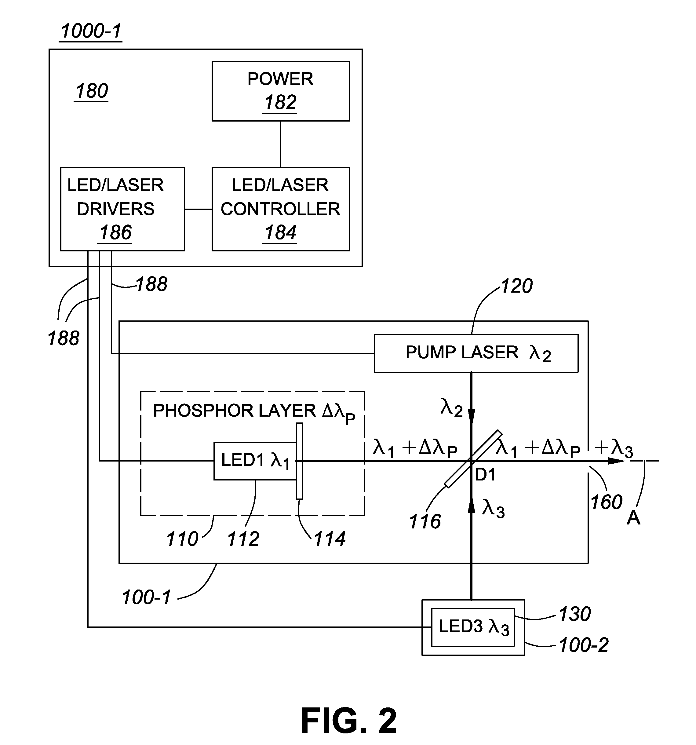
[0063]Thus, a schematic diagram showing elements of an illumination system 1000-1, according to the invention, is shown in FIG. 2. The illumination system 1000-1 comprises a light source unit or module 100-1 for providing high brightness illumination for fluorescence illumination and analysis. The light source unit 100-1 is similar to that shown in FIG. 1, in that it comprises first and second light sources 110 and 120. The first light source 110 comprises an LED 112 (LED1) and a phosphor layer 114, the first LED 112 emitting at a first wavelength λ1 within an absorption band of the phosphor layer and the phosphor layer 114 emitting broadband light emission of longer wavelength, comprising light in a wavelength band ΔλPHOSPHOR (abbreviated as ΔλP in the Figures). The second light source 120 comprises a laser 120, preferably a solid state laser diode, emitting at a second wavelength λ2, also within an absorption band of the phosphor layer. Also provided is a dichroic element, i.e. a ...
third embodiment
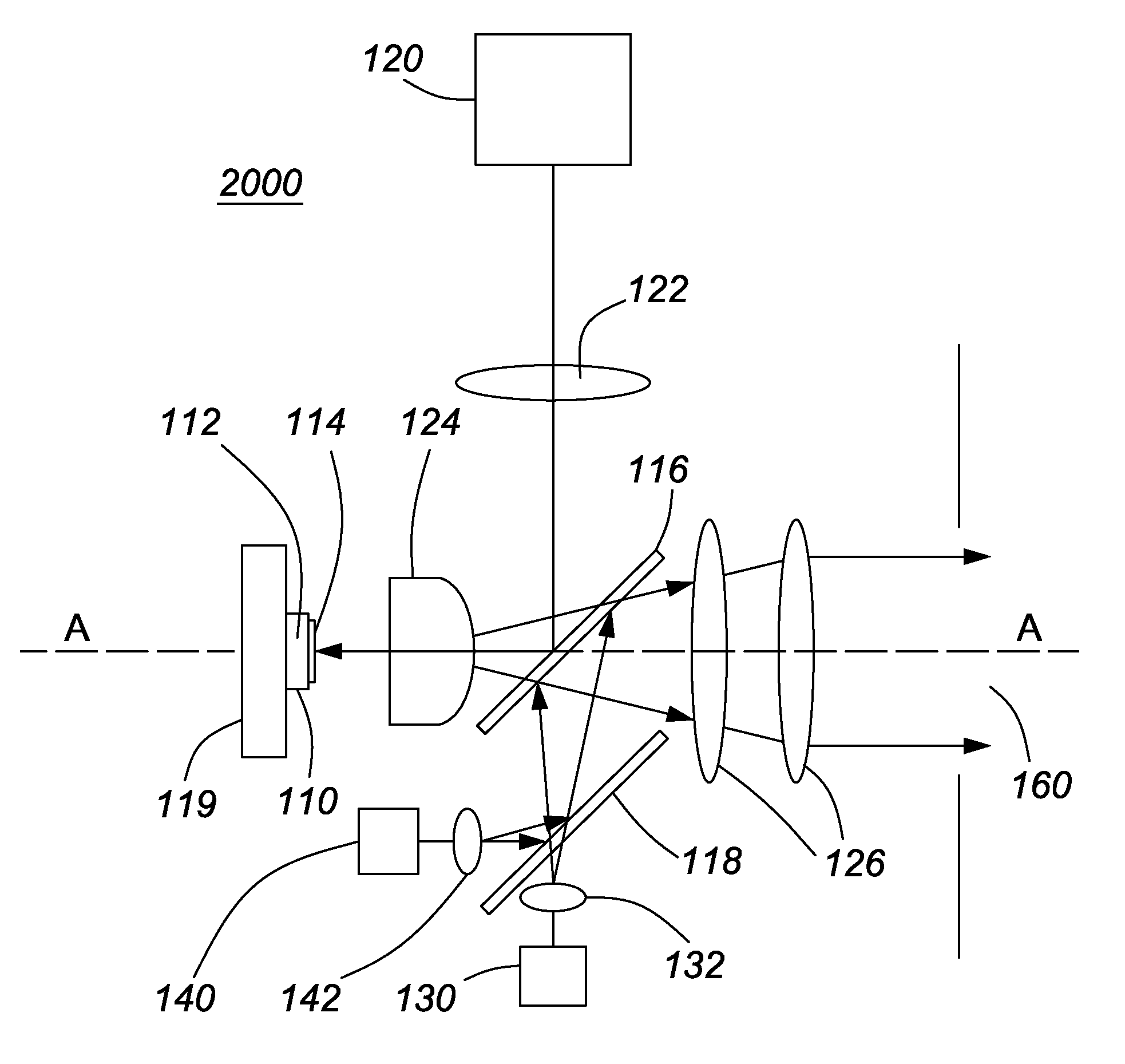
[0069]An illumination system 2000 is shown in FIG. 5. The light source unit 200 comprises a first light source module 100-1, comprising first and second light sources 110 and 120, identical to module 100-1 shown in FIG. 2. Like parts are labeled with the same reference numerals in each Figure. Additionally, a second light source module 100-2 comprises two additional light sources 100-2 and 100-3, i.e. a LED or LED arrays 130 and 140 for light emission at other wavelengths. A second dichroic element, i.e. beam-splitter / combiner 118 is provided, which has a band edge selected to combine the output of LED3 and LED4. That is, a LED 130 (LED3) provides light emission at λ3, and a LED 140 (LED4) provides light emission at wavelength λ4. For example, LED3 and LED4 may provide near ultraviolet (near UV) emission and UV emission respectively.
[0070]The drive system 180 is similar to that shown in FIG. 1, comprising a power supply 182, LED / laser controller 184 and LED / laser drivers 186 for dr...
PUM
 Abstract
Description
Claims
Application Information