

Materials and methods for the preparation of nanocomposites
a technology of materials and composite materials, applied in the field of materials and methods for the preparation of nanocomposites, can solve the problems of insufficient robustness of materials for large-scale advanced material applications, lack of features of materials, and inability to self-assemble materials into superlattices
- Summary
- Abstract
- Description
- Claims
- Application Information
AI Technical Summary
Benefits of technology
Problems solved by technology
Method used
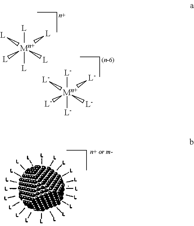
Image

Examples
examples
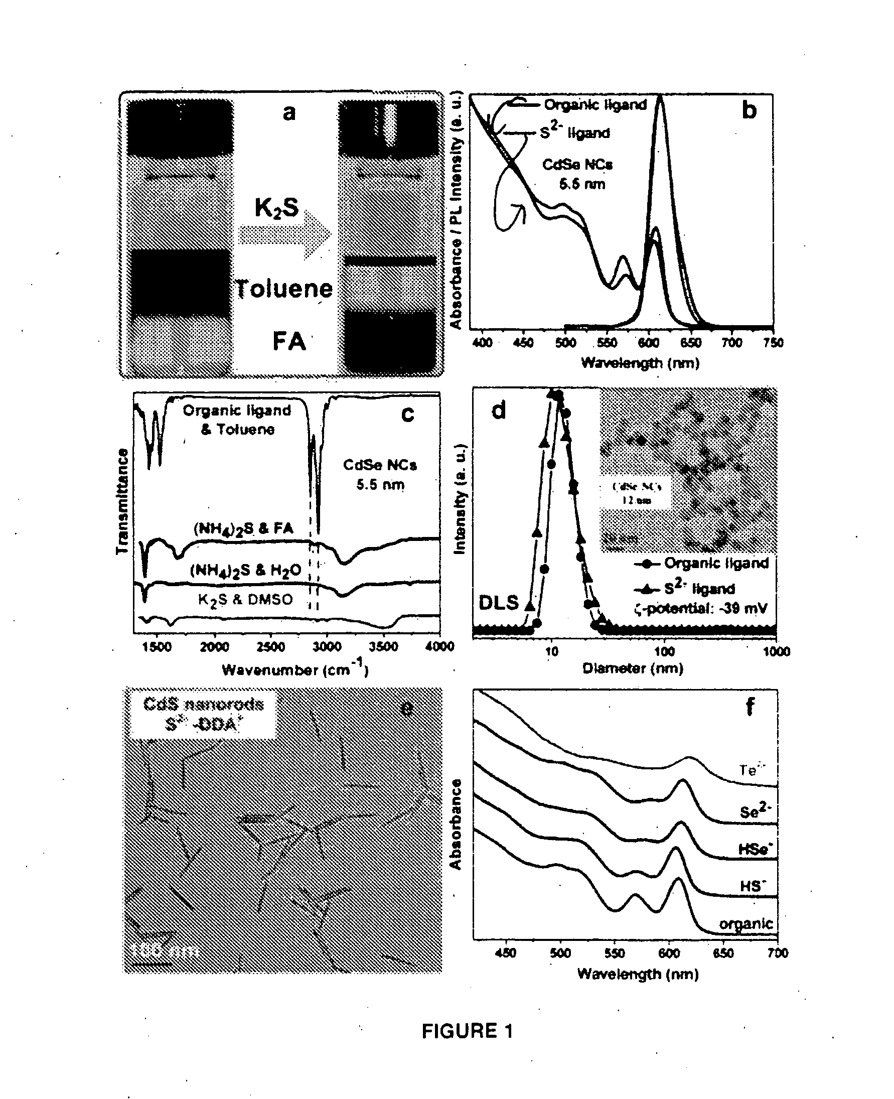
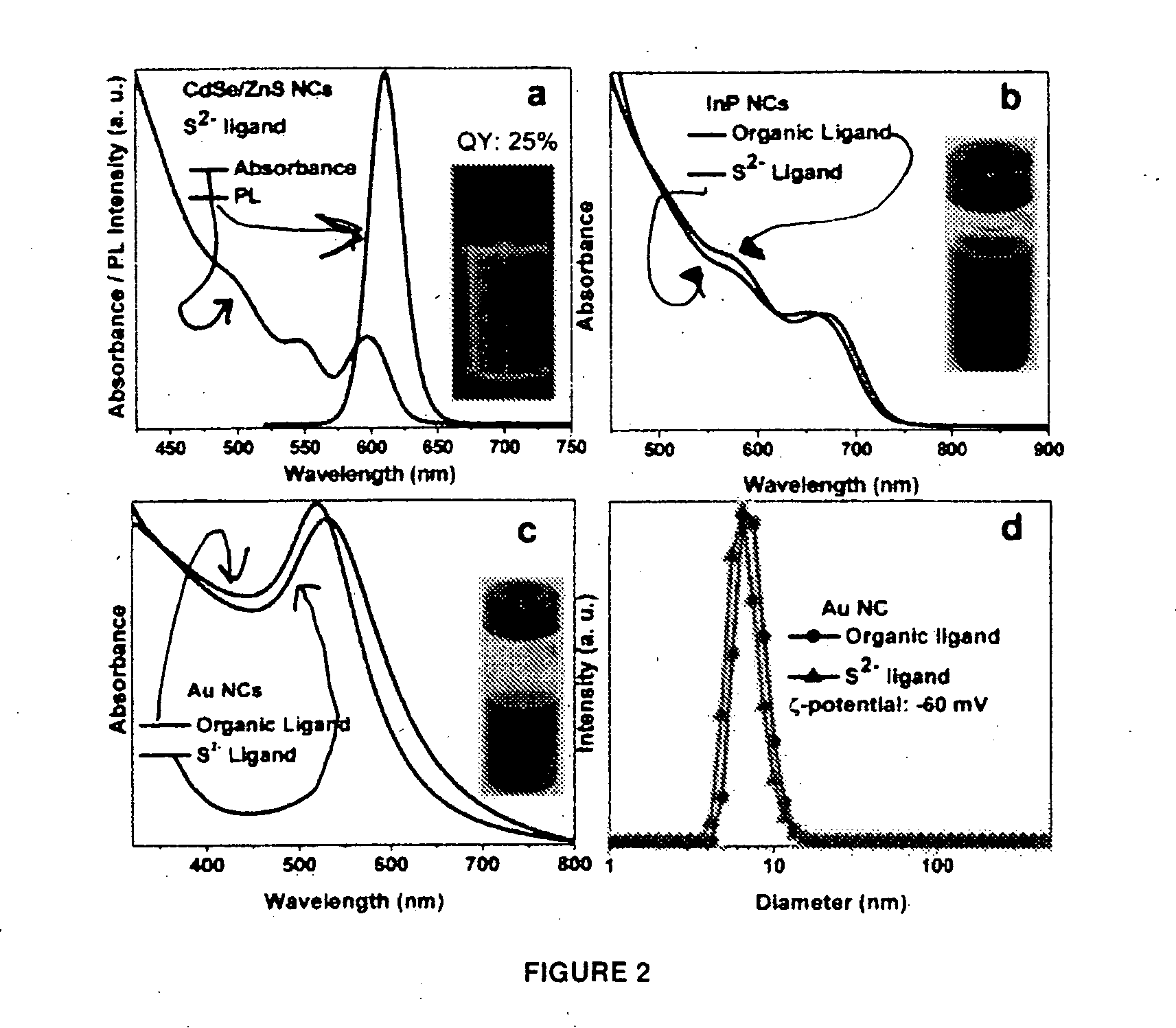
[0213]Chemicals:
[0214]Potassium sulfide (anhydrous, ≧95%, Strem), sodium sulfide nonahydrate (98%, Aldrich), ammonium sulfide (40-48 wt % solution in water, Aldrich), Potassium hydroxide (n0%, Aldrich), Sodium amide (Aldrich), Sulfur (99.998%, Aldrich), Selenium (powder, 99.99%, Aldrich), tellurium (shot, 99.999%, Aldrich), formamide (FA, spectroscopy grade, Aldrich), dimethylsulfoxide (DMSO, anhydrous, 99.9%, Aldrich), acetonitrile (anhydrods, 99.8%, Aldrich), didodecyldimethylammonium bromide (DDAB, 98%, Fluke), Trioctylphosphine oxide (TOPO, 99%, Aldrich), tetradecylphosphonic acid (TDPA, 99%, Polycarbon), octadecylphosphonic acid (ODPA, 99%, Polycarbon), dimethylcadmium (97%, Strem), Cadmium oxide (99.995%, Aldrich), diethylzinc (Aldrich), trioctylphosphine (TOP, 97%, Strem), dodecanethiol (98%, Aldrich), oleylamine (Aldrich), tert-butylamine-borane (97%, Aldrich), InCl3 (99.99%, Aldrich), Indium acetate (99.99%, Alfa Aesar), Al2Se3 (95%, Strem) and Al2Te3 (99.5%, CERAC Inc.).
[0...
PUM
 Abstract
Description
Claims
Application Information