Method for manufacturing silicon substrate having textured structure

Active Publication Date: 2014-11-27
TOKUYAMA CORP
View PDF5 Cites 14 Cited by
  • Summary
  • Abstract
  • Description
  • Claims
  • Application Information

AI Technical Summary

Benefits of technology

[0022]In the method for manufacturing according to the present invention, the concave structure is formed on the silicon substrate surface under the pattern portion and the regular texture structure corresponding to the pattern can easily be formed. The term “pattern portion” used in the present invention means a convex portion that is formed by depositing a resin on the silicon substrate. Specifically, when the resin is printed in the shape of line on silicon substrate, the line is just the “pattern portion”. In the so-called imprinting technology in which concavo-convex structure is formed by applying a resin on a silicon substrate and pressing a mold against the formed resin layer, the convex portion of the concavo-convex structure of resin on the silicon substrate is the “pattern portion”. The expression “concave structure is formed under pattern portion” used in the present invention means that the concave structure is formed substantially over the whole silicon substrate below the respective pattern portions.
[0023]When a pattern of lattice shape or reciprocal lattice shape is formed on a silicon substrate using a composition comprising resin (hereinafter, it may be referred to as “resin-comprising composition”) by, for example, imprint, a concave structure can easily be formed by irradiating an etching gas to the silicon substrate surface other than the pattern portion to remove thin residue portion of coating film other than the pattern portion (refer to as “remaining film”) and by processing then the silicon substrate irradiated with the etching gas with an alkaline etching liquid to etch the silicon substrate surface under the pattern portion of lattice or reciprocal lattice shape. When a pattern of line and space shape is formed on a silicon substrate using a resin-comprising composition, a prism structure can easily be formed by operating similarly.
[0024]According to the method of the present invention, it is not necessary to use silicon substrate having surface oxide film, which is generally used as silicon substrate in manufacture of semiconductor circuit, as shown in the NPL 2 and a silicon substrate which is not subjected to a process of forming surface oxide film can be used just as it is. In the method described in NPL 2, the concave structure is formed on a zone other than the resist pattern formed on t

Problems solved by technology

Accordingly, the texture structure has a defect that the concave and convex are not even.
In case of the etching with the acid etching liquid or the alkaline etching liquid, there is a limit in improvement of power generation efficiency, because it is impossible to form the texture structure in which the concavo-convex structure arranges finely and regularly with the size of less than few μm (micrometer).
In case of forming regular texture structure on silicon substrate surface, among the above-described technologies, imprinting technology is especially focused, because it has a possibility to enlarge area and to form easily and costly a p

Method used


Image

  • Method for manufacturing silicon substrate having textured structure
  • Method for manufacturing silicon substrate having textured structure
  • Method for manufacturing silicon substrate having textured structure

Examples


example 1

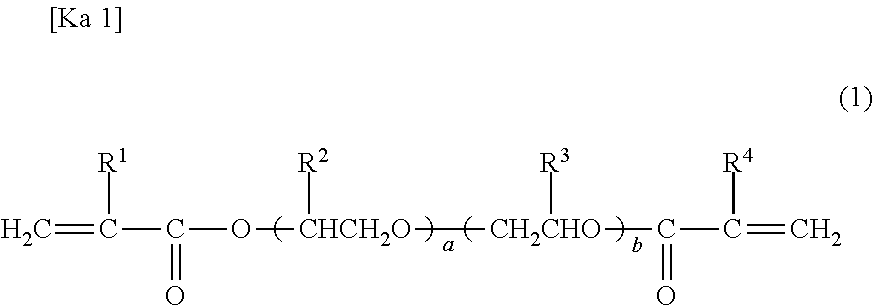
Preparation of Resin-Comprising Composition

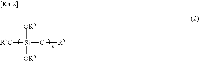
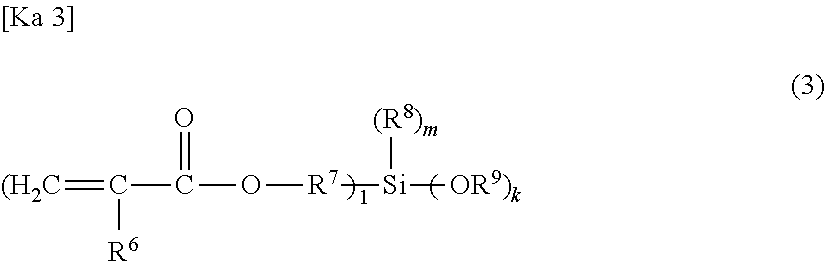
[0173]13.6 g of ethanol, 3.0 g of trimethoxysilylpropyl acrylate as the (meth)acrylic group-containing alkoxysilane, 6.8 g of ethyl silicate 40 (COLCOAT CO., LTD.; on average, pentamer of tetraethoxysilane) as the general alkoxysilane and 1.7 g of 85 wt. % zirconium butoxide (tetrabutyl zirconium alkoxide) in 1-butanol were blended. To the resulting mixture, an aqueous 2N—HCl / ethanol mixed solution which consists of 4.25 g of ethanol, 0.85 g of water and 0.16 g of 2N—HCl was gradually added in drops at room temperature with stirring. Moreover, aqueous ethanol solution which consists of 1 g of ethanol and 0.46 g of water was added gradually in drops and the resulting mixture was stirred at room temperature for one hour to obtain a hydrolysate (c) of mixture of the general alkoxysilane, the (meth)acrylic group-containing alkoxysilane, and the metal akloxide.

[0174]As the polymerizable monomer having (meth)acrylic group (a), 2.5 g of polyoethyl...

example 2

[0186]Operating in the same manner as Example 1, the preparation of resin-comprising composition and the transcription and photo-curing of pattern were conducted.

[0187]The obtained nanoimprint pattern was subjected to the dry etching with oxygen gas for 8 minutes to remove the remaining film.

[0188]A sample having nanoimprint pattern formed under the same condition was observed with SEM to confirm that the remaining was removed.

[0189]Then, operating in the same manner as Example 1, the alkaline etching process and the rinsing treatment were conducted. The SEM photograph after the rinse treatment is shown in FIG. 9 (surface). It was also confirmed that the silicon substrate having the inverted pyramid structure having about 3 μm of one side was manufactured as a silicon substrate having texture structure.

example 3

[0190]13.6 g of ethanol, 3.0 g of trimethoxysilylpropyl acrylate as the (meth)acrylic group-containing alkoxysilane, and 6.8 g of ethyl silicate 40 (COLCOAT CO., LTD.; on average, pentamer of tetraethoxysilane) as the general alkoxysilane were blended. To the resulting mixture, an aqueous 2N—HCl / ethanol mixed solution which consists of 4.25 g of ethanol, 0.85 g of water and 0.16 g of 2N—HCl was gradually added in drops at room temperature with stirring. Moreover, aqueous ethanol solution which consists of 1 g of ethanol and 0.32 g of water was added gradually in drops and the resulting mixture was stirred at room temperature for one hour to obtain a hydrolysate (c) of mixture of the general alkoxysilane and the (meth)acrylic group-containing alkoxysilane.

[0191]Operating in the same manner as Example 1, the polymerizable monomer having (meth)acrylic group (a), the photoinitiator (b), the polymerization inhibitor were homogeneously blended to prepare a mixture and 4 g was weighed from...


PUM


Abstract

The present invention provides a method for manufacturing a silicon substrate having texture structure, by which, in comparison with conventional methods, it is possible to reduce manufacturing step and form easily regular texture structure on silicon substrate surface. The method of the present invention comprises the steps of: (A) forming a pattern on the silicon substrate using a resin-comprising composition; (B) irradiating an etching gas to the silicon substrate surface other than the pattern portion; and (C) processing the silicon substrate irradiated with the etching gas with an alkaline etching fluid to form concave structure under the pattern portion. Furthermore, the present invention provides a resin-comprising composition usable in the method, in particular, a composition comprising photo-curable resin.

Description

TECHNICAL FIELD[0001]The present invention relates to a method for manufacturing a silicon substrate having texture structure in which concave structure is formed selectively under patter portion (in this specification, the term “texture structure” means a “structure having fine concavo-convex shape”). The present invention relates also to a composition comprising resin (hereinafter, it may be referred to as “resin-comprising composition”), which is usable in the above-described method, especially a composition comprising photo-curable resin. According to the present invention, it is possible to form easily a texture structure (inverted pyramid structure) which is suitable for silicon wafer of substrate for solar cell or LED, for example, prism structure, or optional concavo-convex structure which is derived from a pattern. The silicon substrate manufactured by the method, in which the concave portion is formed selectively on portions of the substrate corresponding to the pattern po...

Claims


Application Information

Patent Timeline
IPC IPC(8): H01L21/308
CPCH01L21/3085H01L21/3081B82Y10/00B82Y40/00G03F7/0002G03F7/0047G03F7/027G03F7/0757H01L31/02363Y02E10/50
Inventor UMEKAWA, HIDEKIMATSUI, SHINJIOMOTO, SHINYA
Owner TOKUYAMA CORP
Why Eureka
Try Eureka