Patterning device

a technology of a patterning device and a ring, which is applied in the field of patterning devices, can solve the problems of limited methods in the minimum amount of volume, high cost of inkjet systems, and inability to achieve high-speed printing, and achieve the effect of facilitating the movement towards and inside the hydrophilic elements

Inactive Publication Date: 2014-12-25
KATHOLIEKE UNIV LEUVEN
View PDF0 Cites 25 Cited by
  • Summary
  • Abstract
  • Description
  • Claims
  • Application Information

AI Technical Summary

Benefits of technology

[0029]13. The method, according to any one of the embodiments 1 to 11, whereby the suspended micro- and nanoparticles are magnetic and their movement towards and inside of the hydrophilic elements is facilitated by placing a magnet underneath the hydrophilic elements and thereby accelerates trapping of magnetic particles in the hydrophilic elements and facilitating t...

Problems solved by technology

Usually, these methods are restricted in minimum amount of volume that they are able to dispense and the throughput that is achieved.
Moreover, inkjet systems are usually expensive and the printing of very large arrays is time-consuming.
The classical selection procedure is still lengthy, with weeks to months needed to generate a new aptamer and requiring multiple rounds of selection.
Furthermore, kinetic biases are known limitations of the system because the single representation of a given aptamer sequence among the billions of available sequences not only requires cyclic enrichment to isolate that particular single copy but als...

Method used


Image

  • Patterning device
  • Patterning device
  • Patterning device

Examples


example 1

On Single Crystal Array Formation

[0117]An aqueous NaCl solution (5 M) or was transported 20 times over an array of hydrophilic-in-hydrophobic micropatches, resulting in an array of single NaCl crystals (FIG. 4).

example 2

Fabrication of an Array for Printing of Oligonucleotides and Aptamer Selection

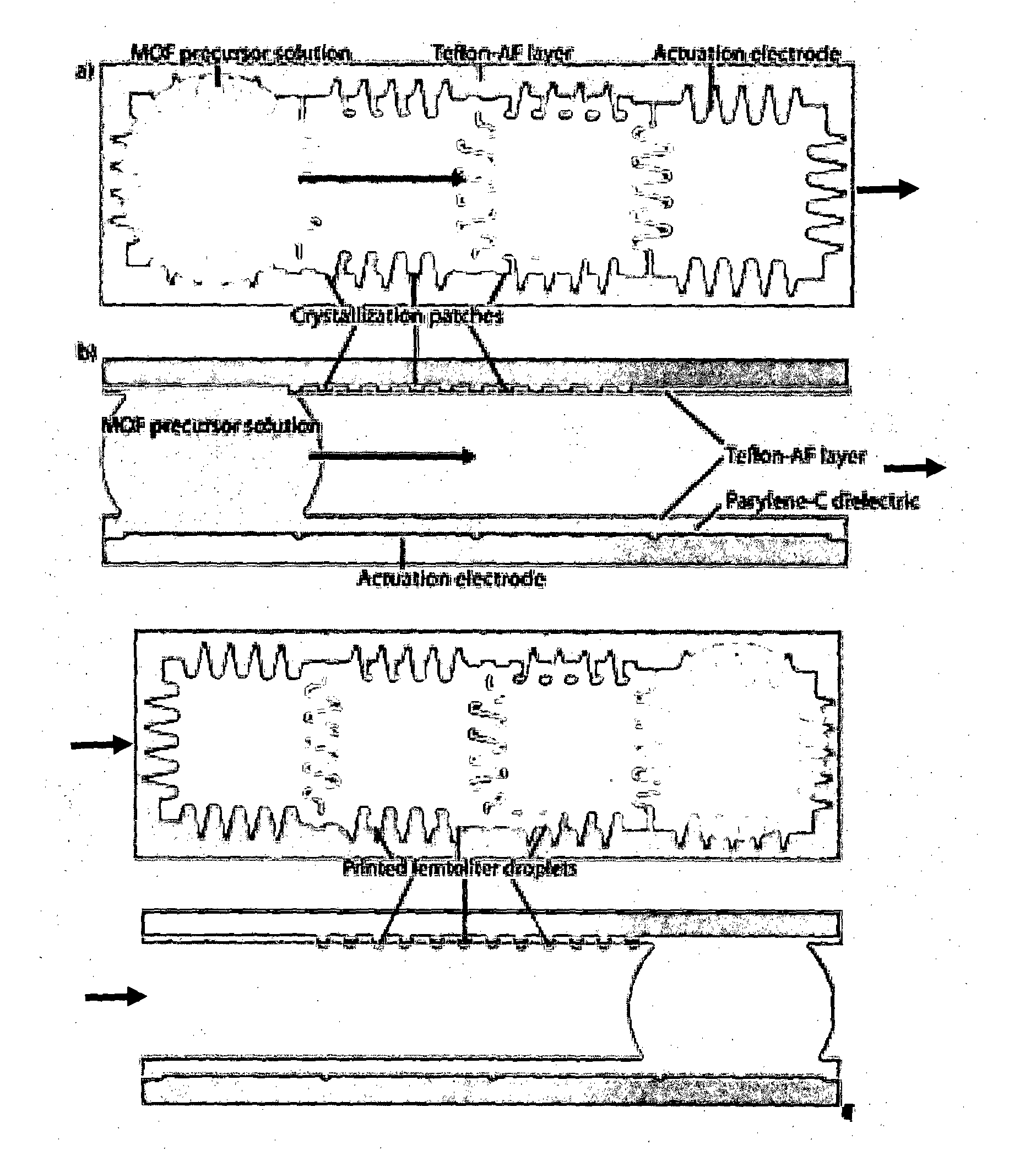
[0118]Digital microfluidic chips are fabricated as follows: glass wafers are cleaned in acetone and isopropyl alcohol for 5 minutes. A thin layer of chromium (100 nm) is then deposited by magnetron sputtering (Balzers BAE 370, Pfaffikon, Switzerland). The chromium layer is patterned by standard photolithographic processes using 51818 positive photoresist, chrome-on-glass photomasks, and wet etching using Cyantec CR-7 chromium etchant. Next, chips are cleaned in 02-plasma (150 mtorr, 100 W) and primed with silane A174 before being coated with a layer of Parylene-C (3 μm) which was deposited using chemical vapor deposition (AL 200, Plasma Parylene Coating Services, Rosenheim, Germany). A thin layer of TEFLON-AF® (˜200 nm thickness, 3% w / w in Fluorinert FC-40) is subsequently spincoated (1200 rpm) on top of the Parylene-C layer, and baked for 5 minutes at 110° C., and 5 minutes at 200° C. Crenellated actuatio...

example 3

Hydrophilic-in-Hydrophobic Microwells

[0167]Hydrophilic-in-hydrophobic microwells were fabricated as follows. Glass slides were coated with TEFLON-AF® to a thickness of 3.25 μm. Next, a thin Parylene-C membrane (500 nm) was deposited on top of the TEFLON-AF® surface by using chemical vapor deposition. Subsequently, an aluminum hard mask (50 nm thickness) was deposited on top of the polymeric stack by thermal evaporation. This aluminum hard mask was patterned by standard photolithography and wet etching to obtain an array of circular features having 4 μm diameter. The exposed areas of the protective Parylene-C mask and TEFLON-AF® were then etched with reactive ion etching using 02-plasma before the protective Parylene-C mask was removed by mechanical peeling.

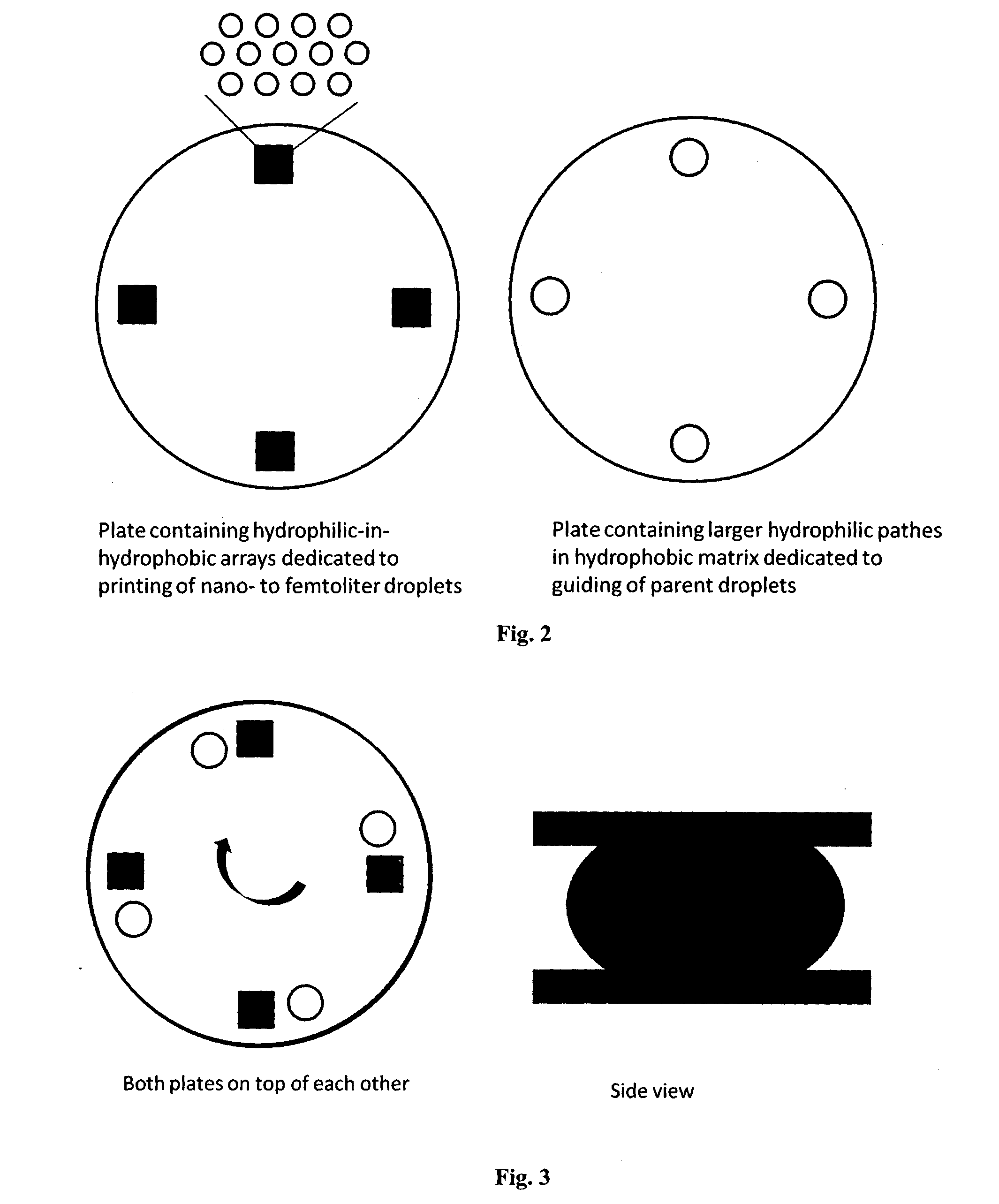
[0168]The glass slide containing these hydrophilic-in-hydrophobic micropatterns was subsequently used as a top plate of a double-plate digital microfluidic chip based on electrowetting-on-dielectric (FIG. 8).

[0169]For demonstratin...


PUM


Abstract

A novel miniaturized and highly automated method for the controlled printing of large arrays of nano- to femtoliter droplets is presented by actively transporting mother droplets over hydrophilic-in-hydrophobic micropatches. The proposed technology consists of single plate or double-plate devices where mother droplets can be actuated and hydrophilic-in-hydrophobic micropatches on one or both plates of the device where nano- to femtoliter droplets are printed. Due to the selective wettability of the more wettable hydrophilic micropatches in a hydrophobic matrix, large nano- to femtoliter droplet arrays are created when mother droplets are transported over these arrays. The parent droplets can be moved by different droplet actuation principles, for example, by using the principle of electrowetting-on-dielectric droplet actuation. We propose another method that uses two plates that are placed on top of each other while being separated by a spacer. One plate is dedicated to confirming and guiding of parent droplets by using hydrophilic patches in a hydrophobic matrix, while the other plate contains hydrophilic-in-hydrophobic arrays dedicated to the printing of nano- to femtoliter droplets. When the plate dedicated to parent droplet guiding is rotated over the plate dedicated to printing of nano- to femtoliter droplets, nano- to femtoliter droplets are dispensed inside the hydrophilic-in-hydrophobic array due to their selective wettability. All these proposed methods allow the parent droplets to be moved over the hydrophilic-in-hydrophobic arrays many times, providing unique advantages for performing bio-assays or miniaturized materials synthesis in nano- to femtoliter sized droplets. Upon the controlled evaporation of the dispensed droplets of solution, large arrays of the printed material can be generated on an automated way in seconds of time on a very flexible way. The method disclosed herein provides a distinct nano- to femtoliter droplet printing technique for a wide variety of applications such as protein- or cell-based bio-assays or printing of crystalline structures, suspensions of nanoparticles or components for microelectronics.

Description

CROSS-REFERENCE TO RELATED APPLICATIONS[0001]This application is a national phase entry under 35 U.S.C. §371 of International Patent Application PCT / BE2013 / 000004, filed Jan. 24, 2013, designating the United States of America and published in English as International Patent Publication WO2013 / 110146 A2 on Aug. 1, 2013, which claims the benefit under Article 8 of the Patent Cooperation Treaty to Great Britain Application Serial No. 1201277.9, filed Jan. 24, 2012, U.S. Provisional Application Ser. No. 61 / 592,399, filed Jan. 30, 2012, Great Britain Application Serial No. 1218994.0, filed Oct. 23, 2012, Great Britain Application Serial No. 1218995.7, filed Oct. 23, 2012, and U.S. Provisional Application Ser. No. 61 / 725,268, filed Nov. 12, 2012, the disclosure of each of which is hereby incorporated herein in its entirety by this reference.BACKGROUND[0002]A. Field of the Disclosure[0003]The disclosure relates generally to a patterning device for printing arrays of nano- to femtoliter dro...

Claims


Application Information

Patent Timeline
IPC IPC(8): B01J19/00
CPCB01J19/0046B01J2219/0065B01J2219/00619B01L3/502707B01L3/502792B01L2200/0668B01L2200/0673B01L2200/142B01L2300/0636B01L2300/0816B01L2300/161B01L2400/0427B01L2400/043B82Y30/00B01J2219/00382B01J2219/00387
Inventor LAMMERTYN, JEROENWITTERS, DAAN
Owner KATHOLIEKE UNIV LEUVEN
Why Eureka
Try Eureka