Radiation resistant CMOS device and method for fabricating the same

a cmos device and radiation resistance technology, applied in the direction of semiconductor devices, electrical devices, transistors, etc., can solve the problems of failure of radiation hardening technology at device level and circuit level, affecting the normal operation of the device, abnormal variation or damage of the logic state of the device, etc., to achieve the effect of improving the charge sharing effect under the single event, improving the device's single event characteristic, and improving the total dose characteristi

Inactive Publication Date: 2015-01-15
PEKING UNIV
View PDF12 Cites 3 Cited by
  • Summary
  • Abstract
  • Description
  • Claims
  • Application Information

AI Technical Summary

Benefits of technology

The present invention provides a new vertical channel CMOS device that can resist total dose radiation and single event radiation in a radiation environment. The device has improved single event characteristics and prevents charge sharing effect. The dielectric protection regions in the semiconductor platform effectively block paths for the source and drain regions collecting charges. The isolation oxide layer prevents the formation of parasite transistors. The dielectric layers disposed under the source region and the drain region can effectively block the diffusing of electrons and holes generated by ionization of the high energy particles.

Problems solved by technology

However, charges trapped in STI regions may turn-on a parasite transistor, which may affect a normal operation of the device.
Moreover, due to a large charge collection region in the silicon substrate, the particles incident on sensitive nodes of the conventional bulk silicon device may cause severe single event effects, causing abnormal variation or damage of logic states of the device.
In addition, the charge sharing effect may bring in failure of the radiation hardening technology at device level and circuit level, such as a protection ring.
However, generally these new device structures can only achieve a single radiation resistance target, rather than targets of resisting a total dose radiation and a single event radiation.
Meanwhile, the charge sharing effect due to the small size is not considered as well.

Method used


Image

  • Radiation resistant CMOS device and method for fabricating the same
  • Radiation resistant CMOS device and method for fabricating the same
  • Radiation resistant CMOS device and method for fabricating the same

Examples


Embodiment Construction

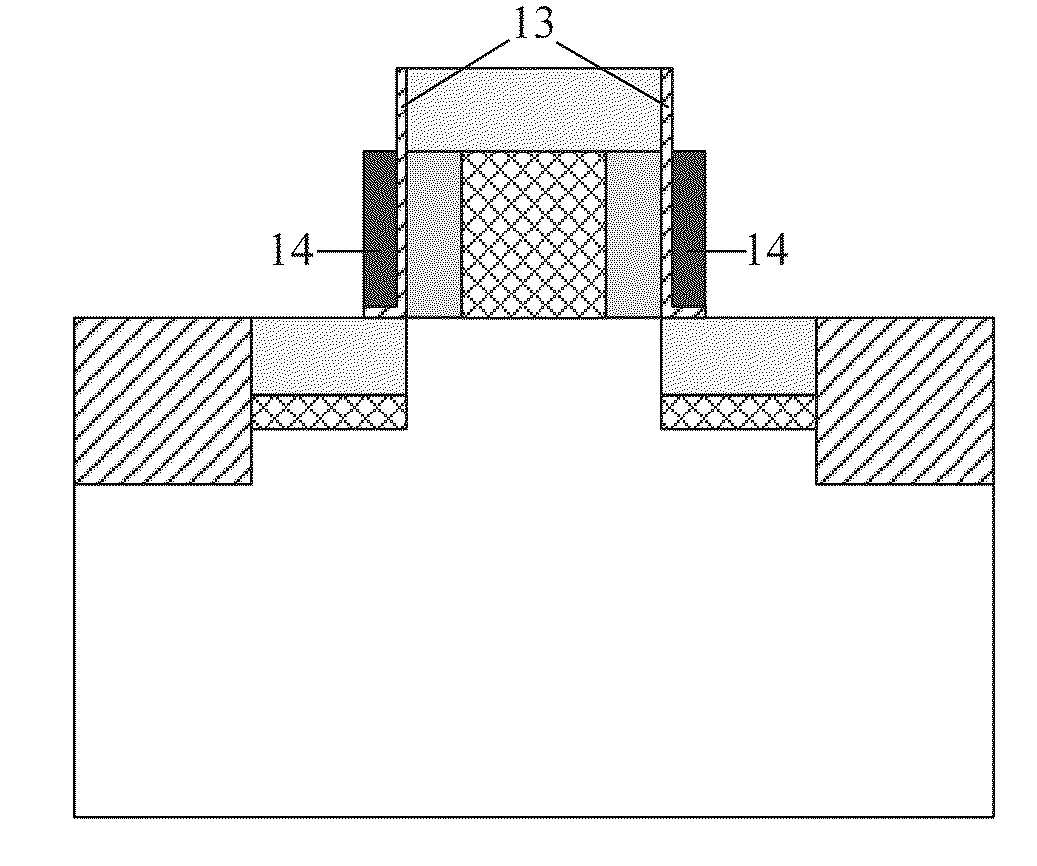
[0025]Hereinafter, an embodiment of the present invention will be described in detail through attached drawings by taking an example of an NMOS, in which a material for a dielectric protection region is silicon nitride.

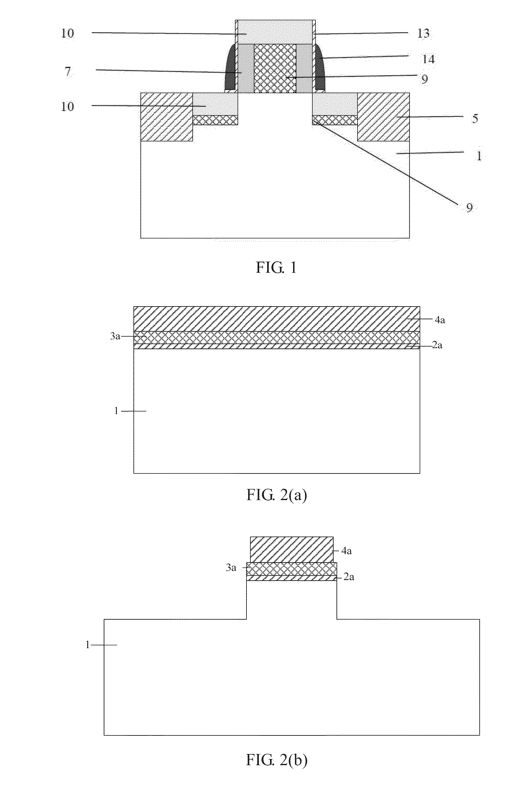
[0026]1) Preparation of a substrate: a P-type (100) silicon substrate 1 is prepared;

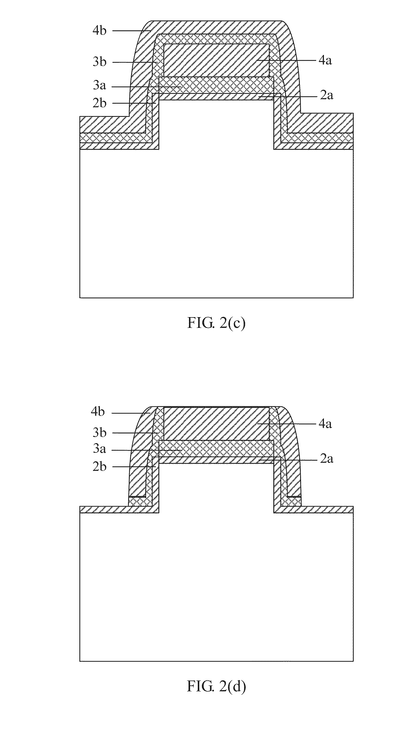
[0027]2) Etching of a silicon platform for an active region: as shown in FIG. 2(a), a silicon dioxide thin layer 2a is formed on the substrate through a thermal oxidation process, a silicon nitride layer 3a is deposited through a low pressure chemical vapor deposition (LPCVD), and then a silicon dioxide layer 4a is deposited through an LPCVD; as shown in FIG. 2(b), a photolithography process is performed, and then the silicon dioxide layer 4a is etched by a reactive ion etching (RIE) process, the silicon nitride layer 3a is etched by a RIE process and the silicon dioxide layer 2a is corroded by hydrofluoric acid, so that the silicon dioxide layer 4a and the silicon nitride layer 3a hav...


PUM


Abstract

A radiation resistant CMOS device and a method for fabricating the same. The CMOS device includes a substrate, a source region, a drain region and a vertical channel on the substrate. A first dielectric protection region is inserted into the vertical channel at the center of the vertical channel to divide the vertical channel into two parts and has a height equal to the length of the vertical channel. The edge of the first dielectric protection region is 20-100 nm from an outer side of the channel, with a central axis of an silicon platform for an active region as the center. A second dielectric protection region is disposed under the source or drain region, with a length equal to the length of the source or drain region and a height of 10-50 nm. The dielectric protection regions effectively block paths for the source and drain regions collecting charges.

Description

CROSS REFERENCE OF RELATED APPLICATIONS[0001]The present application claims priority of Chinese application No. 201210289276.7, filed on Aug. 14, 2012, which is incorporated herein by reference in its entirety.FIELD OF THE INVENTION[0002]The present invention refers to CMOS integrated circuit technologies, and in particular, refers to a radiation resistant CMOS device and a method for fabricating the same.BACKGROUND OF THE INVENTION[0003]Rapid development and wide application of information technologies have changed conventional ways of production, business, management and life, and have brought profound influences on various aspects of human society. With the development of science and technology, especially space technology, nuclear power and nuclear weapon, the relationship between a nuclear radiation environment and an electrical technology are increasingly intimate. In order to meet the requirement for radiation resistance performance of the integrated circuits needed by the de...

Claims


Application Information

Patent Timeline
Patent Type & Authority Applications(United States)
IPC IPC(8): H01L27/092H01L21/8238H01L29/66H01L29/778
CPCH01L29/7788H01L27/092H01L29/66666H01L21/8238H01L21/823814H01L21/823828H01L21/823885H01L29/66636H01L29/7827
Inventor HUANG, RUTAN, FEIAN, XIAWU, WEIKANGHUANG, LIANGXI
Owner PEKING UNIV
Why Eureka
Try Eureka