Copper Foil with Carrier, Method of Producing Same, Copper Foil with Carrier for Printed Wiring Board, and Printed Wiring Board

a technology of copper foil and carrier, which is applied in the manufacture of circuit precursors, electrolytic inorganic material coatings, and metal pattern materials. it can solve the problems of low mechanical strength of thin copper foil, failure of insulation between circuit patterns, and tear or wrinkles during the production of printed circuit boards. achieve excellent effect, increase the adhesion strength with resin, and high peel strength

Active Publication Date: 2015-02-19
JX NIPPON MINING& METALS CORP
View PDF12 Cites 25 Cited by
  • Summary
  • Abstract
  • Description
  • Claims
  • Application Information

AI Technical Summary

Benefits of technology

[0063]As described above, the copper foil with a carrier for a printed wiring board of the present invention includes acicular or rod-like fine roughening particles on at least one surface of the copper foil, instead of the roundish or spherical projections that have been conventionally believed to be good for roughening treatment.
[0064]The copper foil has an excellent effect of increasing the adhesion strength with resin to provide high peel strength to a substrate for package in chemical treatment during fine-pattern formation and thereby allowing fine etching of a printed wiring board. The copper foil with a carrier is also useful for a method of increasing adhesion strength with a copper plating layer for a circuit (electroless plating layer) subsequently formed on a surface of a resin by once removing a copper layer completely to transfer a roughened surface to the resin. In recent increases in fineness of printed circuit patterns and in frequency, the copper foil with a carrier for a printed circuit board of the present invention is significantly effective as a copper foil for a printed circuit (copper foil for a semiconductor package substrate) or a substrate for semiconductor package composed of a copper foil for a semiconductor package substrate and a resin for semiconductor package bonded to each other.

Problems solved by technology

Such an ultra-thin copper foil has low mechanical strength to readily cause tear or wrinkles during production of printed circuit boards.
However, if such an ultra-thin copper layer having such an increased profile such as unevenness and roughness is applied to a semiconductor package substrate, which is a printed wiring board being particularly required to have a fine circuit pattern, unnecessary copper particles remain during circuit etching to cause defects such as insulation failure between circuit patterns.
However, the roundish projections are detached at the time of etching, causing a phenomenon called “powder fall.” Since the contact area between the spherical projection and a copper foil is very small compared to the diameter of the roundish or spherical projection, the phenomenon inevitably occurs.
This has an effect of preventing “powder fall”, but has disadvantages, that is, an increase in the number of steps and a variation in the effect of preventing “powder fall” depending on the thin copper plating.
Consequently, such a layer is unsuitable for a stable circuit design.

Method used


Image

  • Copper Foil with Carrier, Method of Producing Same, Copper Foil with Carrier for Printed Wiring Board, and Printed Wiring Board
  • Copper Foil with Carrier, Method of Producing Same, Copper Foil with Carrier for Printed Wiring Board, and Printed Wiring Board

Examples


example 1

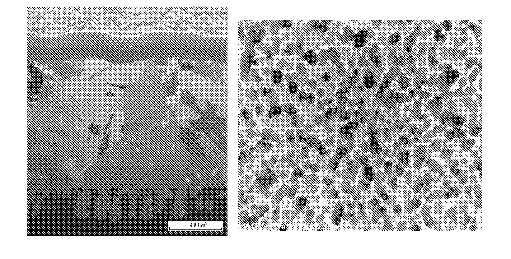
[0196]The rough surface (mat surface: M surface) of a copper foil with a carrier (thickness of ultra-thin copper layer: 5 μm, roughness Rz of roughness-forming surface of ultra-thin copper layer: 0.6 μm) treated as described above was subjected to roughening plating as follows. The treatment conditions are shown below. These are all steps for forming the roughened layer in the copper foil of the present invention. The ratio of current density to limiting current density during roughening particle formation was adjusted to 2.50.

[0197](Liquid Composition 1)[0198]Cu: 15 g / L[0199]H2SO4: 100 g / L[0200]W: 3 mg / L[0201]Sodium dodecyl sulfate amount: 10 ppm

[0202](Electroplating temperature 1): 50° C.

[0203]After the roughening treatment, normal plating shown below was performed. The treatment conditions were as follows.

[0204](Liquid Composition 2)[0205]Cu: 40 g / L[0206]H2SO4: 100 g / L

[0207](Electroplating temperature 1): 40° C.

[0208](Electric Current Condition 1)[0209]Current density: 30 A / dm2 [...

example 2

[0231]The rough surface (mat surface: M surface) of a copper foil with a carrier (thickness of ultra-thin copper layer: 5 μm, roughness Rz of roughness-forming surface of ultra-thin copper layer: 0.6 μm) treated as described above was subjected to roughening plating as follows and to normal plating as in Example 1. The treatment conditions for the roughening plating are shown below. These are all steps for forming the roughened layer of the copper foil of the present invention. The ratio of current density to limiting current density during roughening particle formation was adjusted to 3.10.

[0232](Liquid Composition 1)[0233]Cu: 15 g / L[0234]H2SO4: 100 g / L[0235]W: 3 mg / L[0236]Sodium dodecyl sulfate amount: 10 ppm

[0237](Electroplating temperature 1): 50° C.

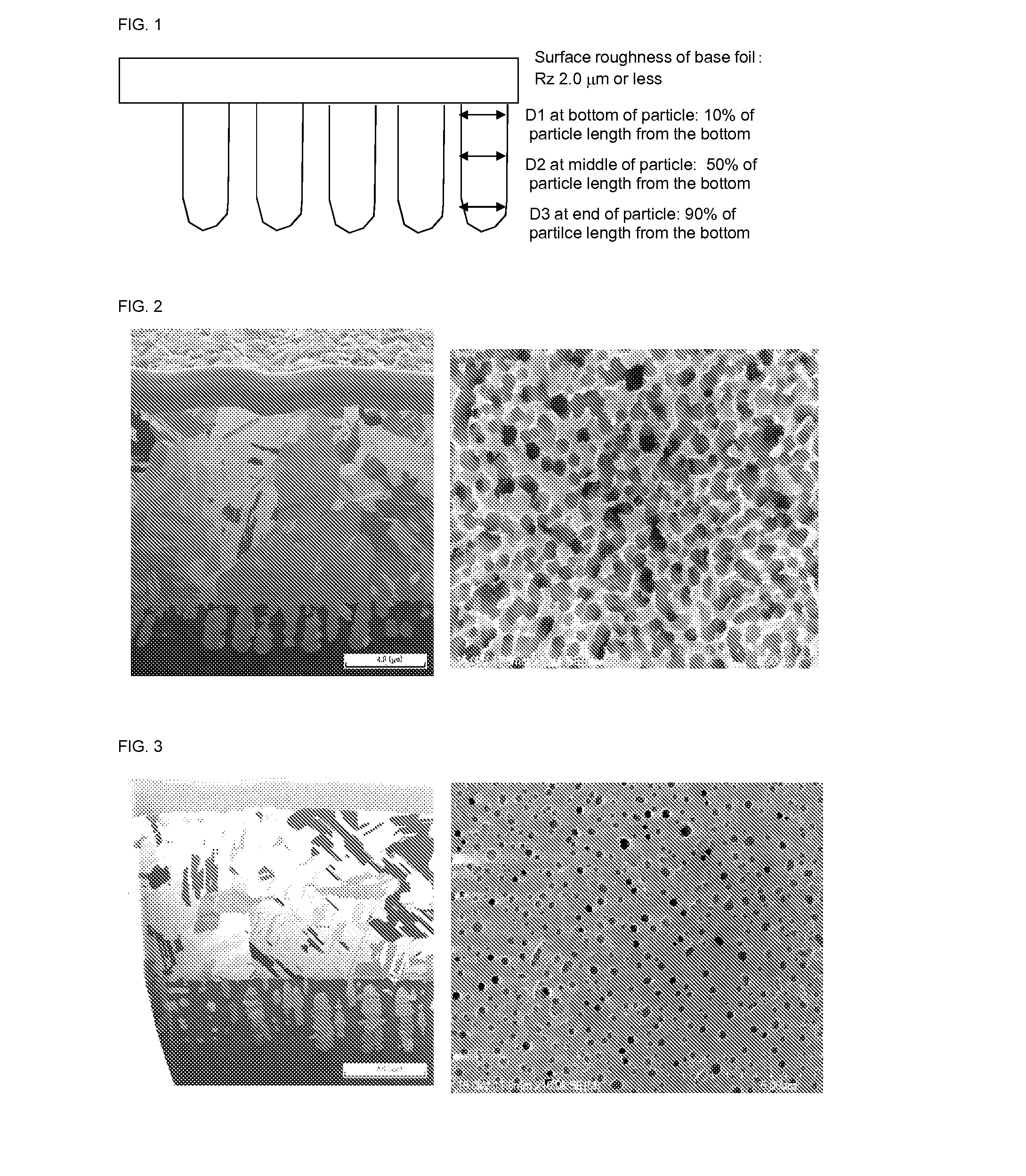
[0238]In this roughened layer, the surface roughness Rz was 1.51 μm, the average diameter D1 at the particle bottom being apart from the bottom of each particle by 10% of the particle length was 0.51 μm, the particle length L1 was 2....

example 3

[0244]The rough surface (mat surface: M surface) of a copper foil with a carrier (thickness of ultra-thin copper layer: 5 μm, roughness Rz of roughness-forming surface of ultra-thin copper layer: 0.6 μm) treated as described above was subjected to roughening plating as follows and to normal plating as in Example 1. The treatment conditions for the roughening plating are shown below. These are all steps for forming the roughened layer of the copper foil of the present invention. The ratio of current density to limiting current density during roughening particle formation was adjusted to 4.30.

[0245](Liquid Composition 1)[0246]Cu: 15 g / L[0247]H2SO4: 100 g / L[0248]W: 3 mg / L[0249]Sodium dodecyl sulfate amount: 10 ppm

[0250](Electroplating temperature 1): 50° C.

[0251]In this roughened layer, the surface roughness Rz was 1.56 μm, the average diameter D1 at the particle bottom being apart from the bottom of each particle by 10% of the particle length was 0.59 μm, the particle length L1 was 2....


PUM

PropertyMeasurementUnit
length L1aaaaaaaaaa
diameter D2aaaaaaaaaa
diameter D3aaaaaaaaaa

Abstract

Provided is a copper foil for a printed wiring board including a roughened layer on at least one surface thereof. In the roughened layer, the average diameter D1 at the particle bottom being apart from the bottom of each particle by 10% of the particle length is 0.2 to 1.0 μm, and the ratio L1/D1 of the particle length L1 to the average diameter D1 at the particle bottom is 15 or less. In the copper foil for printed wiring board, when a copper foil for printed wiring having a roughened layer is laminated to a resin and then the copper layer is removed by etching, the sum of areas of holes accounting for the resin roughened surface having unevenness is 20% or more. The present invention involves the development of a copper foil for a semiconductor package substrate that can avoid circuit erosion without causing deterioration in other properties of the copper foil. In particular, an object of the present invention is to provide a copper foil for a printed wiring board and a method of producing the copper foil, in which the adhesion strength between the copper foil and the resin can be enhanced by improvement of the roughened layer of the copper foil.

Description

TECHNICAL FIELD[0001]The present invention relates to a copper foil with a carrier, a method of producing the copper foil with a carrier, a copper foil with a carrier for a printed wiring board, and a printed circuit board. More specifically, the present invention relates to a copper foil with a carrier to be used as a material for printed wiring boards or shielding materials.BACKGROUND ART[0002]A printed wiring board is generally produced by attaching an insulating substrate to a copper foil to form a copper clad laminate and then forming a conductor pattern on the copper foil surface by etching. Component mounting density and signal frequency have been increased, with the reduction in size and increase in need of high performance of recent electronic devices, and printed wiring boards have been required to have highly fine (fine pitch) conductor patterns and to cope with high frequencies.[0003]Recently, the copper foil having a thickness of 9 μm or less, even 5 μm or less is deman...

Claims


Application Information

Patent Timeline
Patent Type & Authority Applications(United States)
IPC IPC(8): H05K3/38H05K3/18H05K3/02H05K3/06H05K1/03H05K1/09
CPCH05K3/381H05K1/0313H05K1/09H05K3/188H05K3/06H05K3/181H05K3/025B32B9/04B32B15/20H05K3/383H05K3/388B32B3/30B32B15/08C22C9/00H05K3/022H05K3/384H05K2201/0355H05K2203/11B32B2307/714B32B2307/306B32B2457/08B32B15/01C25D1/04C25D3/12C25D3/38C25D5/12C25D9/08Y10T428/12549Y10T428/12569Y10T428/12611Y10T428/12792Y10T428/12847Y10T428/12903Y10T428/1291B32B15/015H05K3/24H05K2201/09009
Inventor NAGAURA, TOMOTAKOHIKI, MICHIYAMORIYAMA, TERUMASA
Owner JX NIPPON MINING& METALS CORP
Why Eureka
Try Eureka