
Nanowire semiconductor device partially surrounded by a grating

a technology of nanowire and grating, which is applied in the direction of semiconductor devices, electrical devices, nanotechnology, etc., can solve the problems of incompatibility with constraints, modulation of threshold voltage, and adjustment of geometrical dimensions of nanowire (width and height), so as to improve the electrical performance of the device, improve the effect of electrostatic control and easy to carry ou

Active Publication Date: 2015-07-09
COMMISSARIAT A LENERGIE ATOMIQUE ET AUX ENERGIES ALTERNATIVES
View PDF2 Cites 30 Cited by
  • Summary
  • Abstract
  • Description
  • Claims
  • Application Information

AI Technical Summary

Benefits of technology

This patent describes a semiconductor device that allows for the creation of transistors with a structure close to that of a FinFET transistor, including a channel region formed by at least two nanowires superimposed or arranged next to one another and a gate arranged on two or three sides of the nanowires. This design allows for better electrostatic control and reduces leakage current while still carrying out standard gate etching. The use of dielectric material with a higher relative permittivity than SiO2 further improve the penetration of the electric field lines and enhance the device's performance. This semiconductor device is ideal for use in high-performance and low-consumption logical applications such as smartphones, tablets, and portable PCs. The planar structure of the semiconductor nanowires also makes it easy to carry out and improves the device's electrical performance.

Problems solved by technology

The modulation of the threshold voltage made possible by an adjustment of the geometrical dimensions of the nanowire (width and height) remains however critical and may be incompatible with the constraints linked to good electrostatic control of the transistor, i.e. having a transistor with a low DIBL (“Drain-Induced Barrier Lowering”) and a low slope under the threshold S (“Subthreshold Slope”).
However, even with such a method, the circumference of the nanowires generally remains substantial and consequently, the electrostatic control is not optimal.
However, a disadvantage of this type of transistor is its difficulty in terms of manufacture.
In order to avoid this problem, the gates are often oversized in order to partially overlap the source and drain zones and it is then difficult to reach the dimensions sought for the gate lengths of this type of transistor, for example less than 15 nm.

Method used


Image

  • Nanowire semiconductor device partially surrounded by a grating
  • Nanowire semiconductor device partially surrounded by a grating
  • Nanowire semiconductor device partially surrounded by a grating

Examples


first embodiment

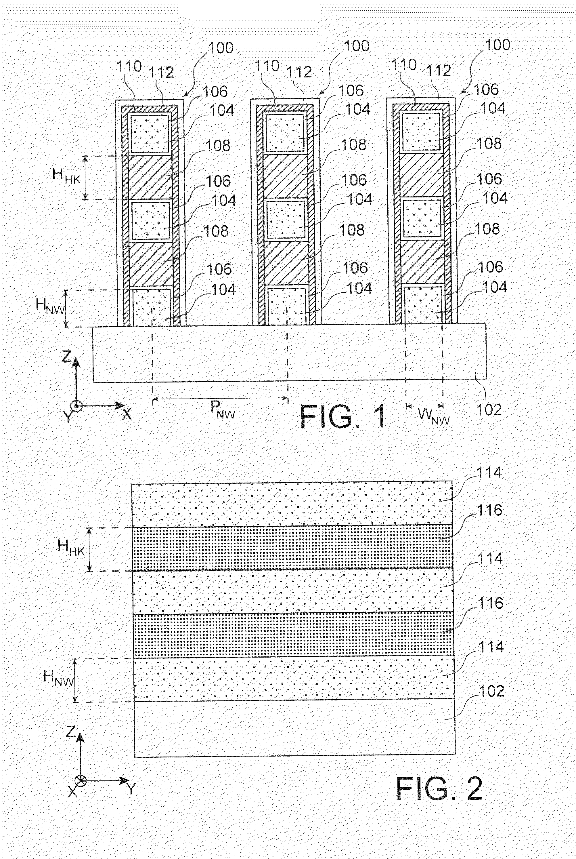
[0072]The semiconductor devices 100 are carried out on a dielectric layer 102 for example comprising an oxide semiconductor such as SiO2. This dielectric layer 102 can itself be arranged on a bulk semiconductor substrate (not shown), for example comprising silicon, or correspond to a buried dielectric layer of a substrate of the semiconductor on insulator type, forming for example a BOX (buried oxide) of an SOI (silicon on insulator) substrate. In the first embodiment described here, the dielectric layer 102 is a thick dielectric layer, with its thickness (dimension according to the axis Z shown in FIG. 1) being for example equal to about 145 nm.

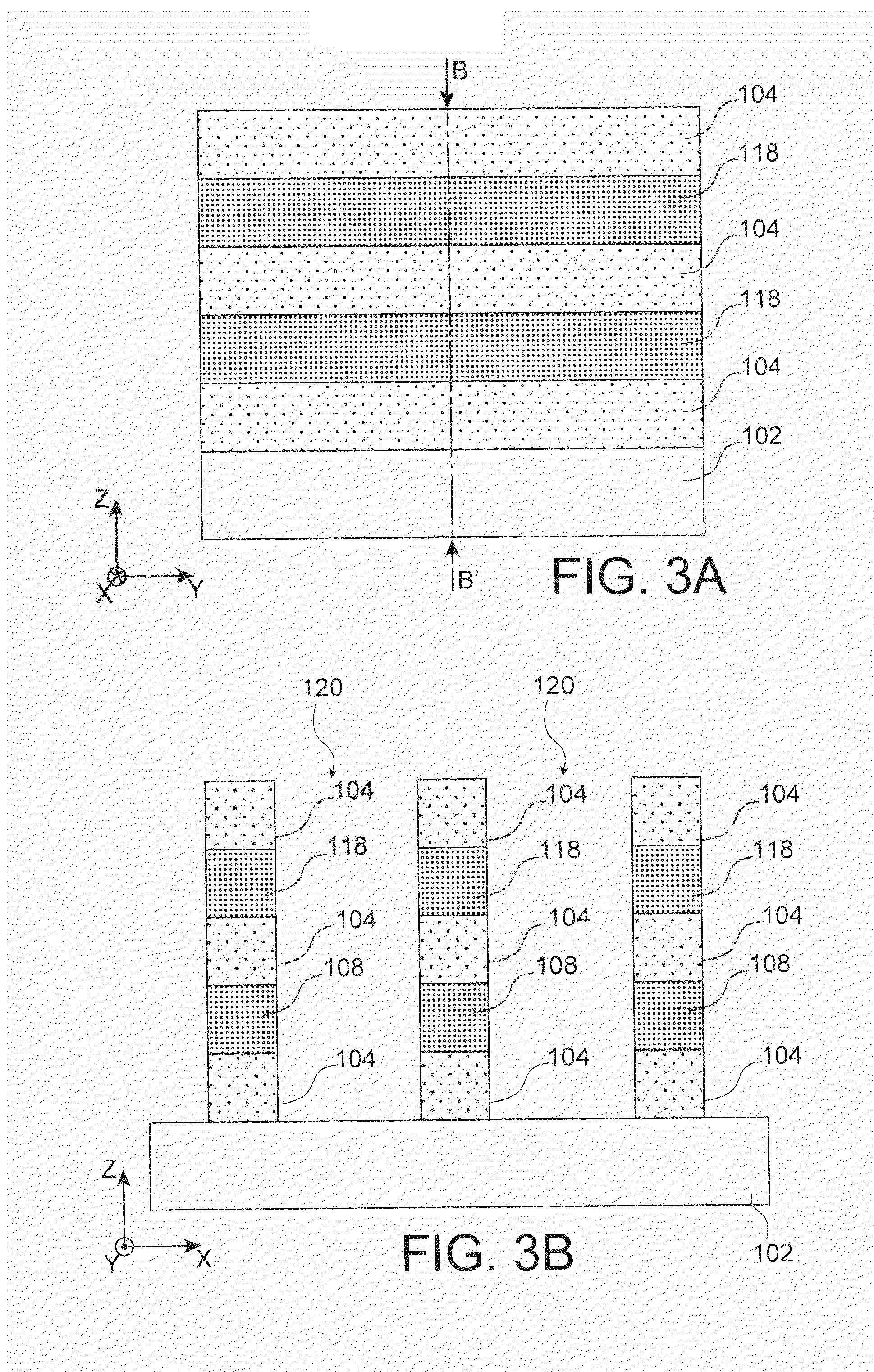
[0073]Each one of the semiconductor devices 100 comprises several semiconductor nanowires 104 (at least two), for example comprising silicon and / or germanium and / or any III-V semiconductor, superimposed one on top of the other and spaced from one another by dielectric structures formed of one or several dielectric materials. In the embodimen...

second embodiment

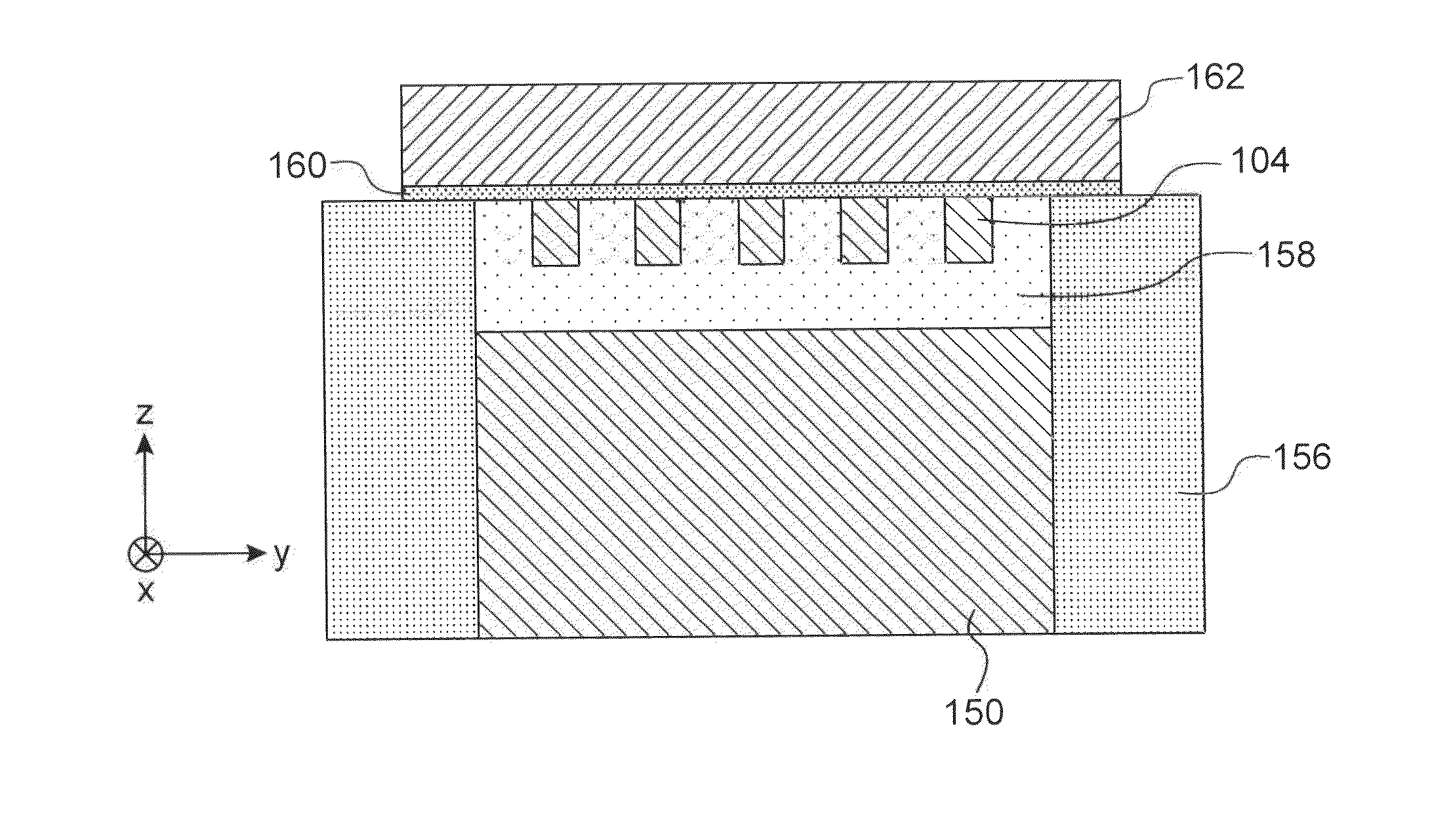
[0104]In relation with FIGS. 8A to 13C, the steps of a method for carrying out a semiconductor device 100 shall now be described, the device 100 corresponding here to a transistor of the FET type comprising nanowires arranged next to one another and spaced one from the other.

[0105]This semiconductor device 100 is carried out using a substrate of the semiconductor on insulator type, for example SOI (silicon on insulator), i.e. comprising a massive semiconductor layer 150, comprising for example silicon and a thickness equal to several hundreds of microns, whereon is arranged a buried dielectric layer 152 (called BOX or “Buried Oxide”) comprising a dielectric material such as SiO2 and a thickness between a few nanometres and a few tens of nanometres, and a superficial layer 154, comprising a semiconductor material such as silicon, germanium, SiGe, or any III-V semiconductor, and arranged on the buried dielectric layer 152. The thickness of the superficial layer 154 (dimension accordi...


PUM


Abstract

A semiconductor device is provided, including two semiconductor nanowires superimposed one on top of the other or arranged next to one another, spaced one from the other and forming channel regions of the semiconductor device, a dielectric structure entirely filling a space between the nanowires and which is in contact with the nanowires, a gate dielectric and a gate covering a first of the nanowires, sidewalls of the nanowires and sidewalls of the dielectric structure when the nanowires are superimposed one on top of the other, or covering a part of the upper faces of the nanowires and a part of an upper face of the dielectric structure when the nanowires are arranged next to one another, and wherein the dielectric structure comprises a portion of dielectric material with a relative permittivity greater than or equal to 20.

Description

TECHNICAL FIELD AND PRIOR ART[0001]A semiconductor device is described here comprising several semiconductor nanowires superimposed or arranged next to one another, spaced one from the other and which are partially surrounded by a gate. This advantageously applies to the carrying out of devices of the FET (Field Effect Transistor) type, in particular for high-performance and low-consumption logic applications in microelectronics. This also applies to the carrying out of MOSFET transistors with nanowires superimposed or arranged next to one another, for example for the carrying out of integrated circuits having improved electrical performance with respect to the circuits of prior art.[0002]The semiconductor nanowires are nanostructures with which it is possible to carry out transistors of the FinFET (“Fin-shaped Field Effect Transistor”, or 3D transistor) type. In such a FinFET transistor, instead of having one active zone corresponding to a planar structure as in a conventional MOSF...

Claims


Application Information

Patent Timeline
IPC IPC(8): H01L29/10H01L29/66H01L21/02H01L29/06H01L21/306H01L29/78H01L29/16
CPCH01L29/1033H01L29/78H01L29/66568H01L21/02603H01L29/0673H01L21/30604H01L21/02532H01L29/16B82Y10/00B82Y40/00H01L29/42364H01L29/66439H01L29/775H01L29/0649H01L29/42392H01L29/66795H01L29/785H01L29/78696
Inventor BARRAUD, SYLVAINRIVALLIN, PIERRETTESCHEIBLIN, PASCAL
Owner COMMISSARIAT A LENERGIE ATOMIQUE ET AUX ENERGIES ALTERNATIVES
Learn More