System and method for picoliter volume microfluidic diagnostics
- Summary
- Abstract
- Description
- Claims
- Application Information
AI Technical Summary
Benefits of technology
Problems solved by technology
Method used
Image
Examples
example 1
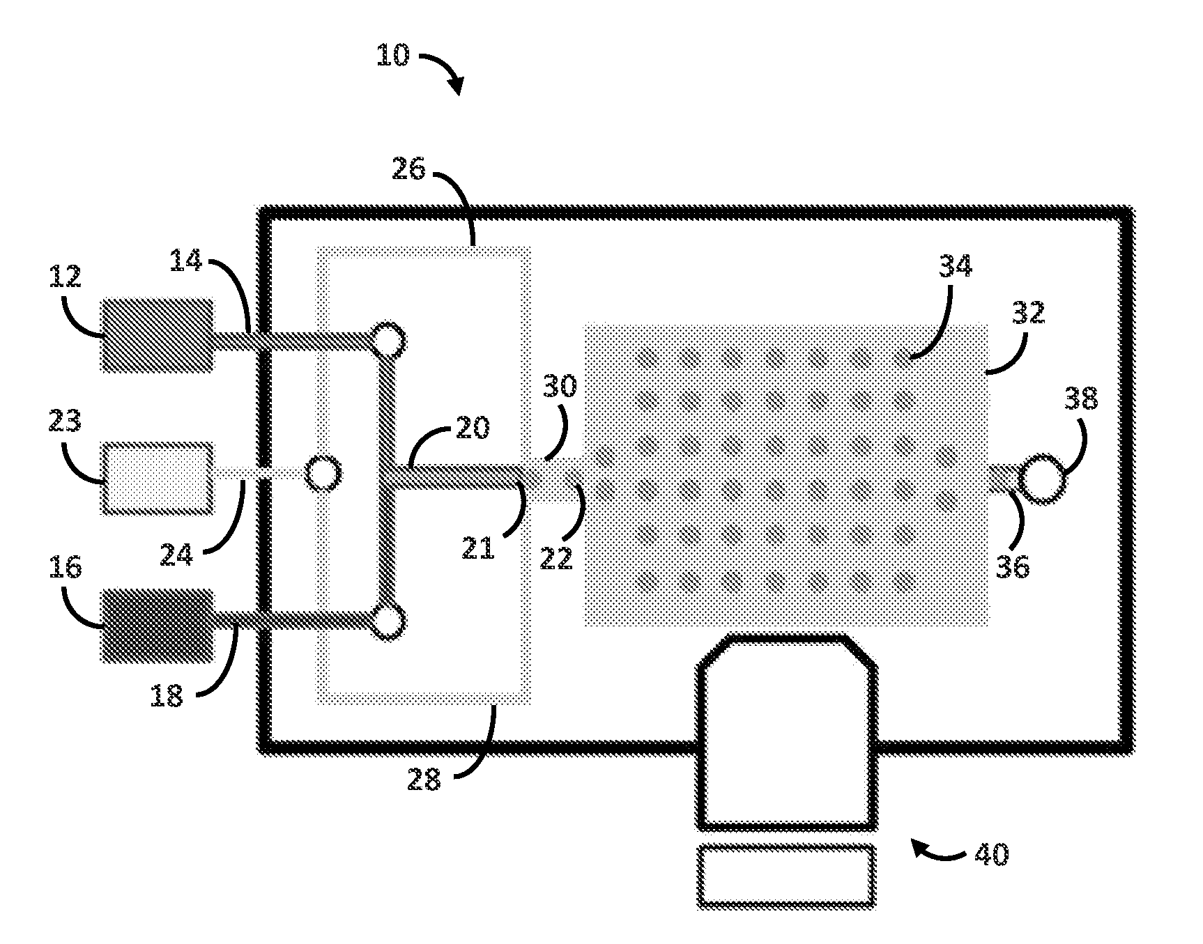
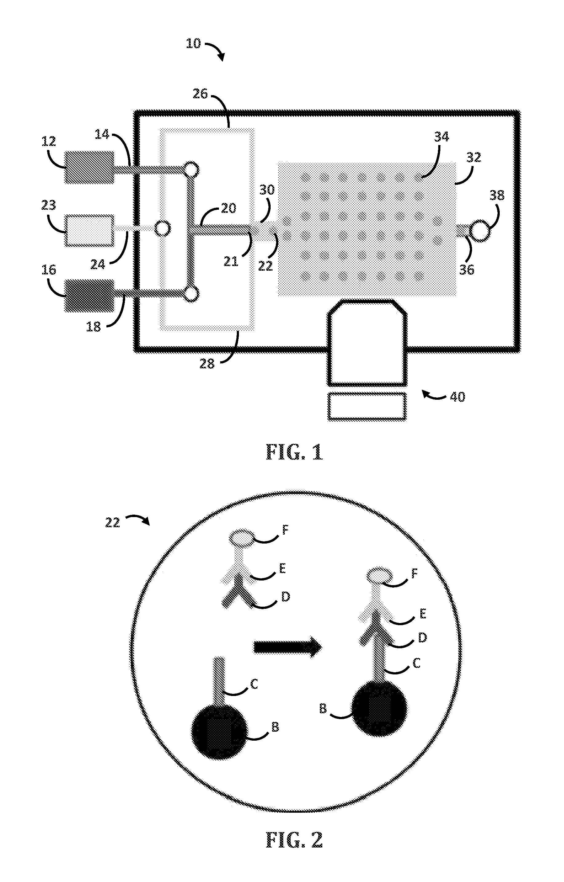
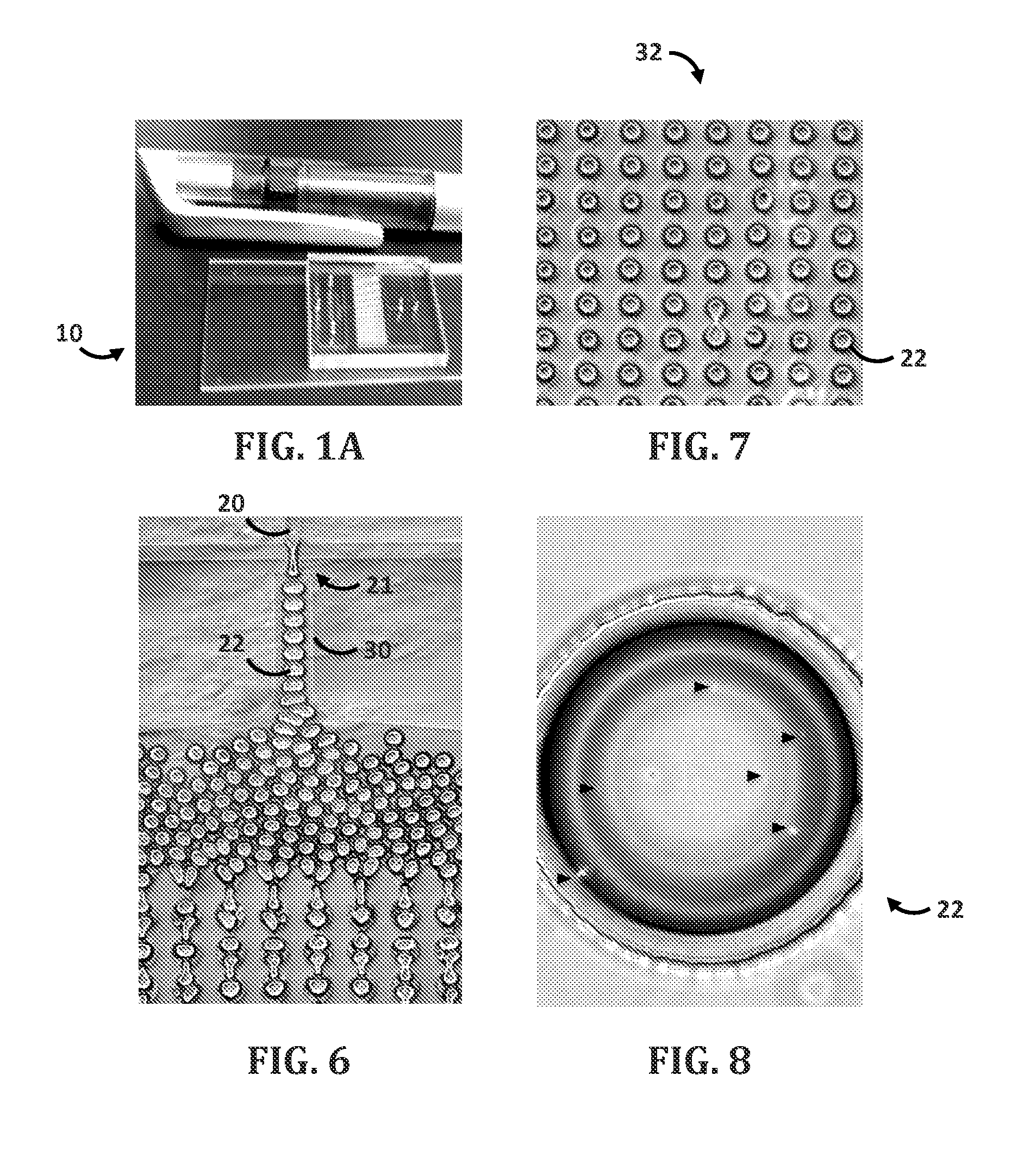
[0096]Droplet microfluidic flow focusing devices were fabricated using soft lithography. Negative photo resist SU-8 2100 (MicroChem, Newton, Mass.) was deposited onto clean silicon wafers to a thickness of 150 μm, and patterned by exposure to UV light through a transparency photomask (CAD / Art Services, Bandon, Oreg.). Sylgard 184 polydimethylsiloxane (PDMS) (Dow Corning, Midland, Mich.) was mixed with crosslinker (ratio 10:1), poured onto the photoresist patterns, degassed thoroughly and cured for 12 h at 75° C. The PDMS devices were peeled off the wafer and bonded to glass slides after oxygen-plasma activation of both surfaces. The microfluidic device was composed of two parts: a droplet forming nozzle (channel cross section 6.25*10−8 m2, FIG. 1) and a 103 droplets storage array (channel cross section 3.13*10−7 m2, FIG. 1). The multi-droplet array provided simultaneous measurement of multiple reactions, thus it decreased the standard error of the mean. On the day of the experiment,...
example 2
[0100]Construction of the optics system included, in part, a custom made, motorized, dual view, computerized portable microscopy system designed for droplet microfluidic imaging (R&D Engineering Solutions, Netania, Israel). The dual view system was used for the simultaneous imaging of the whole chip (top view camera) and specific droplets (bottom view camera). The top view camera included a 1280×768 resolution, color sensor, auto / computer-controlled focus, manually configurable [83×50 mm-30×18 mm] field of view, 640×480 region of interest (ROI), and zoom functionality. The bottom view (microscope) camera was characterized by a 752×582 resolution, monochrome 8.6 μm×8.3 μm pixels sensor, and a 10× objective. A single 3W 468 nm light emitting diode (LED) was used for florescence excitation. A 41017—Endow GFP / EGFP bandpass fluorescence filter set (Chroma Inc., VT) was used for florescence detection. Top illumination was made by a single 30 mW white LED for chip observation and microscop...
example 3
[0106]An example script is provided as follows:
NAMEMicroscope_Experiment_1LOCATIONHome5000, 6000, 2000LOCATIONDest2000, 3000, 4000TRANSFERHomeDest(+5, +10, +20)*51lightonTRANSFERHome+5, +10, +20*53lightonTRANSFERDestDest(+5, +10, +20)*56lighton
[0107]The present invention has been described in terms of one or more preferred embodiments, and it should be appreciated that many equivalents, alternatives, variations, and modifications, aside from those expressly stated, are possible and within the scope of the invention.
[0108]Each reference identified in the present application is herein incorporated by reference in its entirety.
[0109]While present inventive concepts have been described with reference to particular embodiments, those of ordinary skill in the art will appreciate that various substitutions and / or other alterations may be made to the embodiments without departing from the spirit of present inventive concepts. Accordingly, the foregoing description is meant to be exemplary, ...
PUM
 Abstract
Description
Claims
Application Information


