Fusion bonded liquid crystal polymer electrical circuit structure

a liquid crystal polymer and electrical circuit technology, applied in the direction of printed element electric connection formation, liquid/solution decomposition chemical coating, coating, etc., can solve the problems of flexible circuits are expensive compared to some rigid pcb products, and flexible circuits have limitations regarding layer count or feature registration, etc., to achieve high density and routing challenges, reduce manufacturing costs, and reduce the effect of cos

Active Publication Date: 2016-07-21
LCP MEDICAL TECH LLC
View PDF7 Cites 12 Cited by
  • Summary
  • Abstract
  • Description
  • Claims
  • Application Information

AI Technical Summary

Benefits of technology

[0021]The present disclosure permits the creation of circuit structures with lines and spaces below 50 micron, and preferably below 20 microns, and supports signal integrity beyond 40 GHz. The material sets can be processed with conventional circuit fabrication techniques and equipment. The solid metal vias provide superior electrical performance over conventional barrel plated or micro vias. The present disclosure is applicable to rigid, flexible and rigid flex circuits, as well as semiconductor packaging.
[0022]The present disclosure permits bulk conductive material to be added to create a very small low resistance vias to increase density and reduce line, and feature pitch of the high density circuit. The printed circuit can be produced to replicate a traditional circuit, or it can be an interconnect to one or more members of a system embedded or incorporated.

Problems solved by technology

Advances in semiconductor packaging are driving significant density and routing challenges.
Power and thermal management are challenges with low voltage systems to preserve battery life.
In general, flexible circuits are expensive compared to some rigid PCB products.
Flexible circuits also have some limitations regarding layer count or feature registration, and are therefore generally only used for small or elongated applications.
Rigid PCBs and package substrates experience challenges as the feature sizes and line spacing are reduced to achieve further miniaturization and increased circuit density.
As density increases, however, laser processed via structures can experience significant taper, carbon contamination, layer-to-layer shorting during the plating process due to registration issues, and high resistance interconnections that may be prone to result in reliability issues.
The challenge of making fine line PCBs often relates to the difficulty in creating very small or blind and buried vias.
For high speed applications, loss associated with glass weave and solder mask arc an issue, and conventional via technology has become a major source of impedance mismatch and signal parasitic effects.
In general, signal integrity, high aspect ratio vias and line and space requirements limit the relationship between semiconductor packaging and the printed circuit board the chips are mounted to.

Method used


Image

  • Fusion bonded liquid crystal polymer electrical circuit structure
  • Fusion bonded liquid crystal polymer electrical circuit structure
  • Fusion bonded liquid crystal polymer electrical circuit structure

Examples


Embodiment Construction

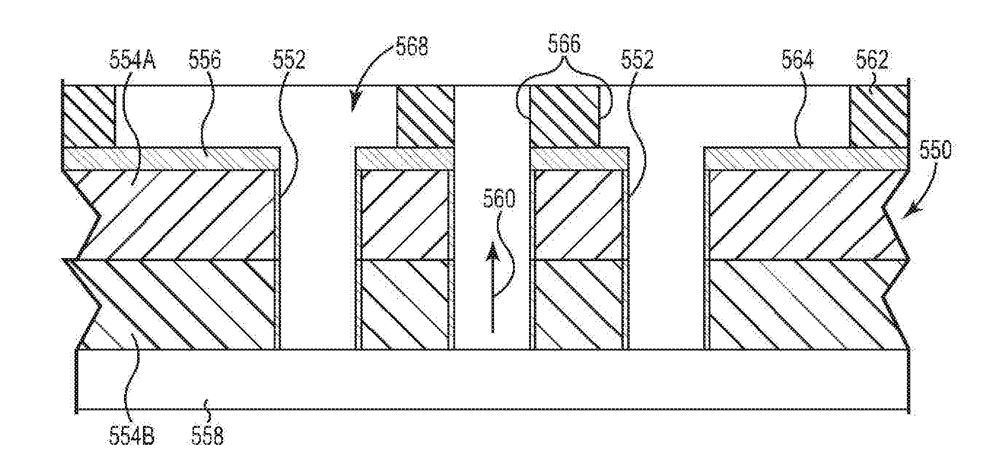
[0050]The present high density circuit structure can be configured as a low cost, high signal performance electrical interconnect assembly, which has a low profile that is particularly useful for desktop and mobile PC applications. In another embodiment, the high density circuit structure can also be a portion of a socket or semiconductor package.

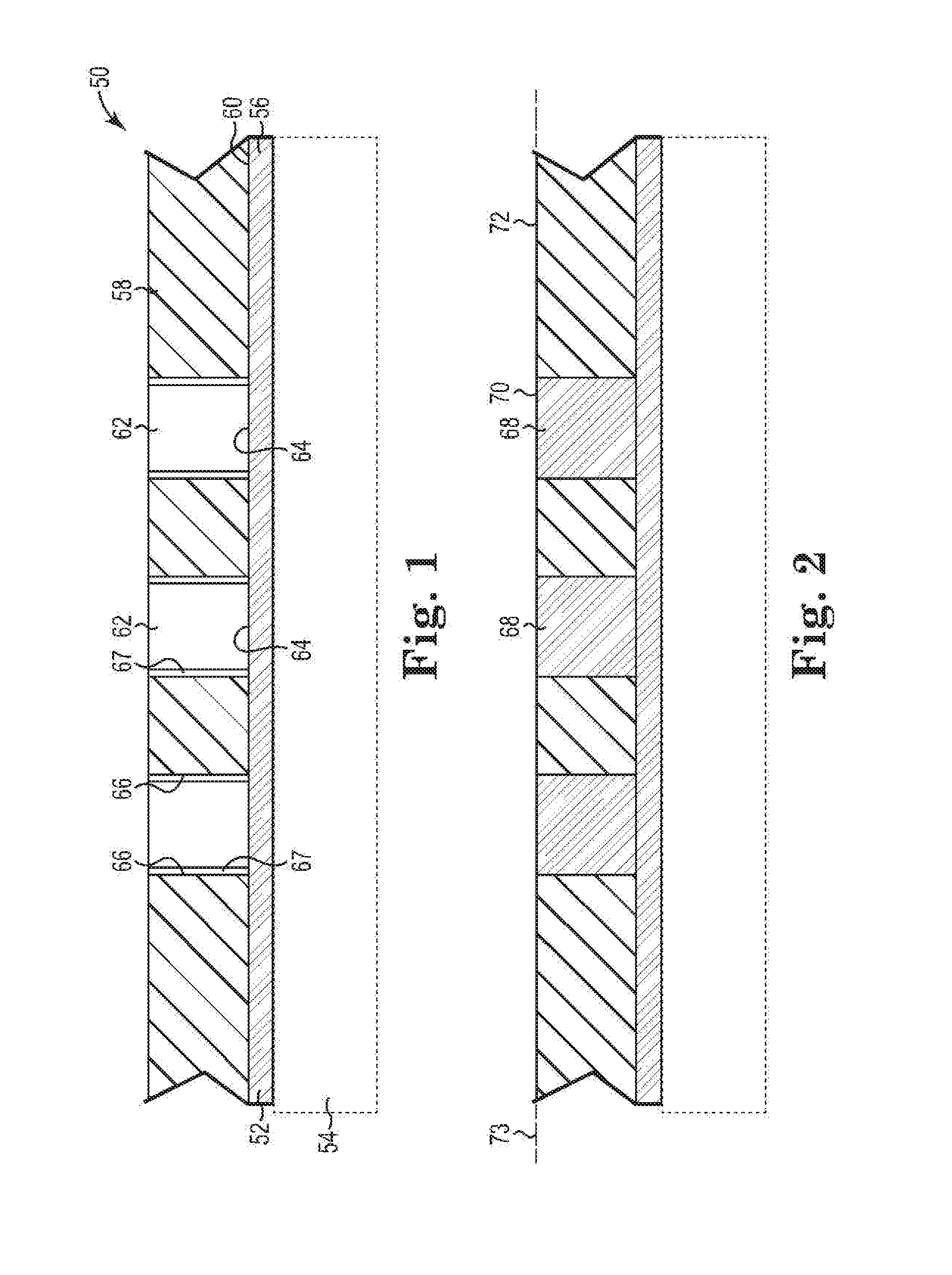
[0051]FIG. 1 is a side cross-sectional view of a method of making the circuit structure 50 in accordance with an embodiment of the present disclosure. A copper foil 52 is preferably supported by base layer 54. The base layer 54 can be a sacrificial member that is removed at some point later in the process.

[0052]If the end product is a flexible circuit, the base layer 54 can be a material such as polyimide or liquid crystal polymer. If the final product is a rigid circuit board, the base layer 54 can be FR4 or one of many high speed laminates or substrates. If the final product is a semiconductor package, the base layer 54 can be a material ...


PUM

PropertyMeasurementUnit
thicknessaaaaaaaaaa
thickaaaaaaaaaa
diameteraaaaaaaaaa

Abstract

A method of making a fusion bonded circuit structure. A substrate is provided with a seed layer of a conductive material. A first resist layer is deposited on the seed layer. The first resist layer is processed to create first recesses corresponding to a desired first circuitry layer. The first recesses expose, portions of the seed layer of conductive material. The substrate is electroplated to create first conductive traces defined by the first recesses. The first resist layer is removed to reveal the first conductive traces. The substrate is etched to remove exposed portions of the seed layer adjacent the first conductive traces. A portion of the seed layer is interposed between the first conductive traces and the substrate. A first layer of LCP is fusion boned to the first major surface of the substrate to encapsulate the first conductive traces in an LCP material. The first LCP layer can be laser drilled to expose the conductive traces.

Description

CROSS-REFERENCE TO RELATED APPLICATIONS[0001]This application claims the benefit of U.S. Provisional Application No. 62 / 140,038, filed Mar. 30, 2015 the entire disclosure of which is hereby incorporated by reference.[0002]This application is a continuant-in-part of U.S. application Ser. No. 14 / 864,215, filed Sep. 24, 2015, entitled Fusion Bonded Liquid Crystal Polymer Circuit Structure, which claims the benefit of a national stage application under 35 U.S.C. 371 of International Application No. PCT / US2014 / 045856, entitled FUSION BONDED LIQUID CRYSTAL POLYMER ELECTRIC CIRCUIT STRUCTURE, filed Jul. 9, 2014, which claims priority to United States Provisional Application Nos. 61 / 845,088, filed Jul. 11, 2013 and 61 / 915,194 filed Dec. 12, 2013, the disclosures of which are hereby incorporated by reference.TECHNICAL FIELD[0003]The present disclosure relates to an electrical circuit structure constructed using a liquid crystal polymer (“LCP”) dielectric material, and a corresponding methods...

Claims


Application Information

Patent Timeline
Patent Type & Authority Applications(United States)
IPC IPC(8): H05K3/46H01L21/48H05K3/00H05K3/40H05K3/18H05K3/06
CPCH05K3/4623H05K3/188H05K3/06H05K3/0026H05K2203/1333H05K3/181H01L21/4857H01L21/486H05K2203/12H05K3/4038C23C18/1603C23C18/1653C23C18/38C25D7/123C25D3/38H01L2224/16225H01L2224/48091H01L2224/48227H01L2924/15311H05K1/0393H05K3/421H05K3/429H05K3/4635H05K3/4679H05K2201/0141H05K2201/09563H01L2924/00014Y10T29/49128
Inventor RATHBURN, JAMES J.
Owner LCP MEDICAL TECH LLC
Why Eureka
Try Eureka