Organometal Halide Perovskite Nanoplatelets, Devices, and Methods
a technology of perovskite nanoplatelets and organic halide, which is applied in the direction of amino preparation from amines, sustainable manufacturing/processing, and final product manufacturing, etc., and can solve the problems of not meeting the performance typical of organic or quantum dot based leds, and no efficient peleds that include perovskite nanoparticles have been demonstrated
- Summary
- Abstract
- Description
- Claims
- Application Information
AI Technical Summary
Benefits of technology
Problems solved by technology
Method used
Image

Examples
example 1
Synthesis of MAPbBr3 Nanoplatelets
[0062]Colloidal nanoplatelets of methylammonium lead bromide (MAPbBr3) perovskite were synthesized by adding 0.1 mmol PbBr2, 0.16 mmol CH3(CH2)7NH2, 0.24 mmol methylamine (33% in absolute ethanol), and 0.5 mmol HBr sequentially into 200 μL DMF to form a mixture precursor solution.
[0063]After the solids were dissolved, the clear precursor solution was added into 3 mL acetone at room temperature, which produced a yellow-green colloidal solution.
[0064]The supernatant was discarded, and a yellow precipitate was collected and air dried after centrifugation at 4400 rpm for 10 min.
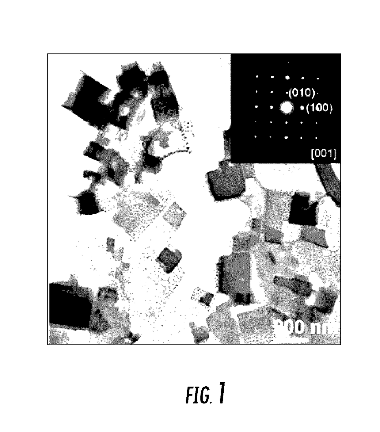
[0065]The MAPbBr3 nanoplatelets were stable in ambient environment with humidity around 55% for at least one week, and were re-dispersed in toluene or acetone before device fabrication. The as-prepared perovskite nanoparticles were substantially single crystalline nanoplatelets with varying size (50×50 to 300×300 nm2) and thickness (indicated by the contrast in the Transmission E...
example 2
Fabrication of Devices
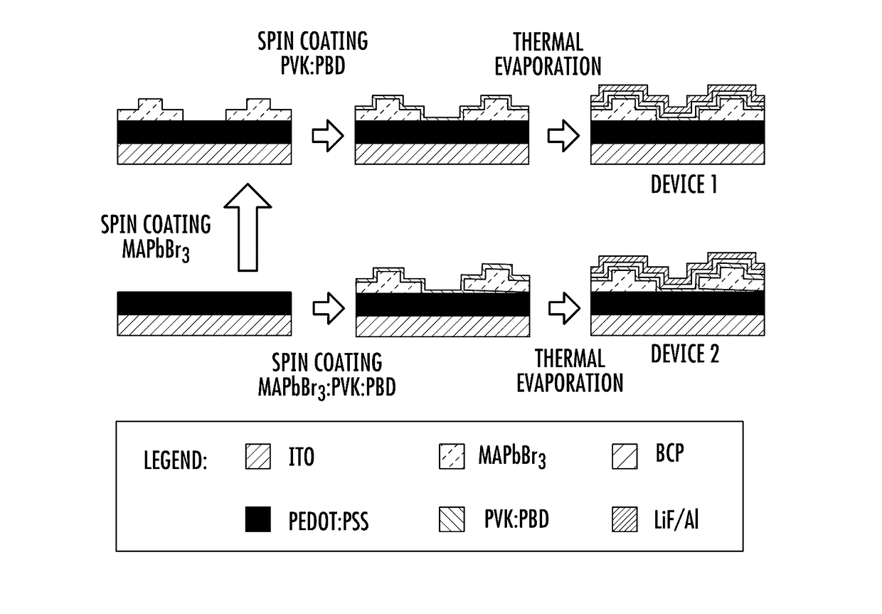
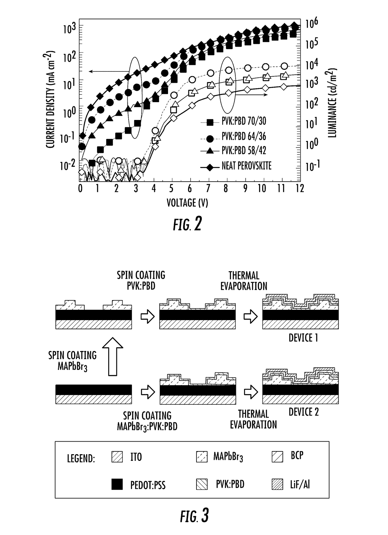
[0066]Using the metal halide perovskite nanoplatelets of Example 1 as a light emitting material, highly efficient LEDs exhibiting bright green EL centered at 530 nm with high color purity (FWHM 20 nm) were produced. A maximum luminance of 10590 cd m−2 was achieved at a voltage of 12 V and a current density of 874 mA cm−2 (FIG. 2), which was more than four times brighter than the current best-performing MAPbBr3 nanoparticle-based LED (2000 cd m−2) (Li G. et al. Nano Lett. 2015, 15, 2640).
[0067]ITO-coated glass substrates were sequentially cleaned by sonication in soap solution; rinsed with deionized water; sonicated in acetone and isopropyl alcohol for 15 min each; and dried with nitrogen gas flow. The substrates then were treated with UV ozone for 20 min prior to use.
[0068]A PEDOT:PSS solution was filtered by a 0.45 μm polytetrafluoroethylene (PTFE) syringe filter prior to use. The PEDOT:PSS solution was spin-coated onto the ITO substrates at 3000 rpm for 40 se...
example 3
Characterization of MAPbBr3 Nanoplatelets and Devices
[0083]Transmission Electron Microscopy: Transmission electron microscopy images were obtained with a JEM-ARM200cF (JEOL USA, Inc., Mass., USA) operated at 200 kV. For conventional TEM studies, the colloidal MAPbBr3 nanoplatelet precursor of Example 1 (20 mg mL−1 in acetone) was spin-coated onto Cu / lacey-carbon TEM grids.
[0084]Atomic Force Microscopy: Atomic force microscopy images were taken with an Icon scanning probe microscope (Bruker, USA) in tapping-mode.
[0085]X-ray Diffraction: The MAPbBr3 nanoplatelet on a glass substrate was characterized by a X'PERT Pro powder X-ray diffractometer (PANalytical, USA). Diffraction patterns were recorded from 10 to 50° 2θ with a step size of 0.02° at 1° min−1.
[0086]The X-ray diffraction (XRD) pattern showed that the nanoplatelets of Example 1 had a cubic lattice structure with a unit cell of 5.93 Å, which was close to that of bulk MAPbBr3 perovskites (FIG. 6). Two satellite peaks by the side...
PUM
| Property | Measurement | Unit |
|---|---|---|
| Quantum yield | aaaaa | aaaaa |
| Nanoscale particle size | aaaaa | aaaaa |
| Nanoscale particle size | aaaaa | aaaaa |
Abstract
Description
Claims
Application Information
 - Generate Ideas
- Intellectual Property
- Life Sciences
- Materials
- Tech Scout
- Unparalleled Data Quality
- Higher Quality Content
- 60% Fewer Hallucinations
Browse by: Latest US Patents, China's latest patents, Technical Efficacy Thesaurus, Application Domain, Technology Topic, Popular Technical Reports.
© 2025 PatSnap. All rights reserved.Legal|Privacy policy|Modern Slavery Act Transparency Statement|Sitemap|About US| Contact US: help@patsnap.com