Ultra long lifetime gallium arsenide

a gallium arsenide and long-life technology, applied in the direction of chemically reactive gases, crystal growth process, polycrystalline material growth, etc., can solve the problems of reduced free-carrier lifetime of materials, low efficiency, high cost, etc., and achieve the effect of increasing the carrier lifetim

Inactive Publication Date: 2017-07-20
BAE SYST INFORMATION & ELECTRONICS SYST INTERGRATION INC
View PDF0 Cites 6 Cited by
  • Summary
  • Abstract
  • Description
  • Claims
  • Application Information

AI Technical Summary

Benefits of technology

[0013]One aspect of an embodiment of the present disclosure relates generally to a new embodiment of bulk GaAs with an increased carrier lifetime of at least 10 microseconds to be used for optical and electrical devices. Another aspect of an embodiment of the present disclosure includes a method for growing gallium arsenide (GaAs) to produce material with ultra-long free carrier lifetimes (>10 microseconds). The method involves using a technique called low pressure hydride vapor phase epitaxy (LP-HVPE). In this technique, GaCl gas is reacted with AsH3 gas at the surface of a GaAs substrate. An epitaxial, high quality, vapor grown GaAs crystal is grown on top of the lower quality GaAs substrate in this manner. The epitaxial, vapor grown crystal is the material possessing the ultra-long free carrier lifetimes.

Problems solved by technology

Commercially available GaAs always has a significant concentration of a defect called EL2 (As on Ga antisite defects) which are known to greatly reduce the free-carrier lifetime of the material.
Historically, however, semiconductor radiation detectors have been limited by high cost, operational complexity, low efficiency due to limited size, and difficulty achieving high-purity, defect-free crystals.
Unfortunately, progress in overcoming these obstacles over the years has been slow and incremental.
Progress in the development of high resolution, room temperature, gamma radiation detectors has been severely limited for many years by the size, quality, and transport properties of single crystal compound semiconductors.
CdxZn1-xTe (CZT) is the most commercially advanced of these materials, but Te inclusions, twins, and grain boundaries are constant barriers to the size, yield, and cost of these crystals for detector applications.
Gallium arsenide (GaAs) has been studied as a radiation detector since the early 1960's, predating CZT, but its widespread use for gamma ray detection has never been realized due to the presence of native deep level traps (EL2, i.e., AsGa antisites) which reduced its free carrier lifetime at room temperature.

Method used


Image

  • Ultra long lifetime gallium arsenide
  • Ultra long lifetime gallium arsenide
  • Ultra long lifetime gallium arsenide

Examples


Embodiment Construction

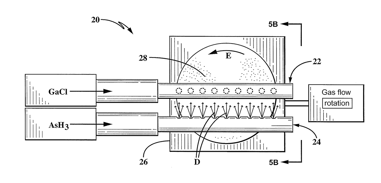
[0029]In accordance with an aspect of the present disclosure, an exemplary embodiment provides a new GaAs with an increased carrier lifetime of at least 10 microseconds that can be used for optical devices, electrical devices and other devices. One particular embodiment of a new GaAs is created using a known, but little-used, method of vapor growth of semiconductor crystals, low pressure hydride vapor phase epitaxy (LP-HVPE), to produce GaAs with the unique properties of having ultra-long free carrier lifetimes. This method of fabricating the preferred embodiment of a new GaAs crystal significantly advances the state of the art of semiconductor materials for multiple applications, including high resolution radiation detectors, dramatically improves the material quality, and is scalable to production of large quantities and aperture sizes.

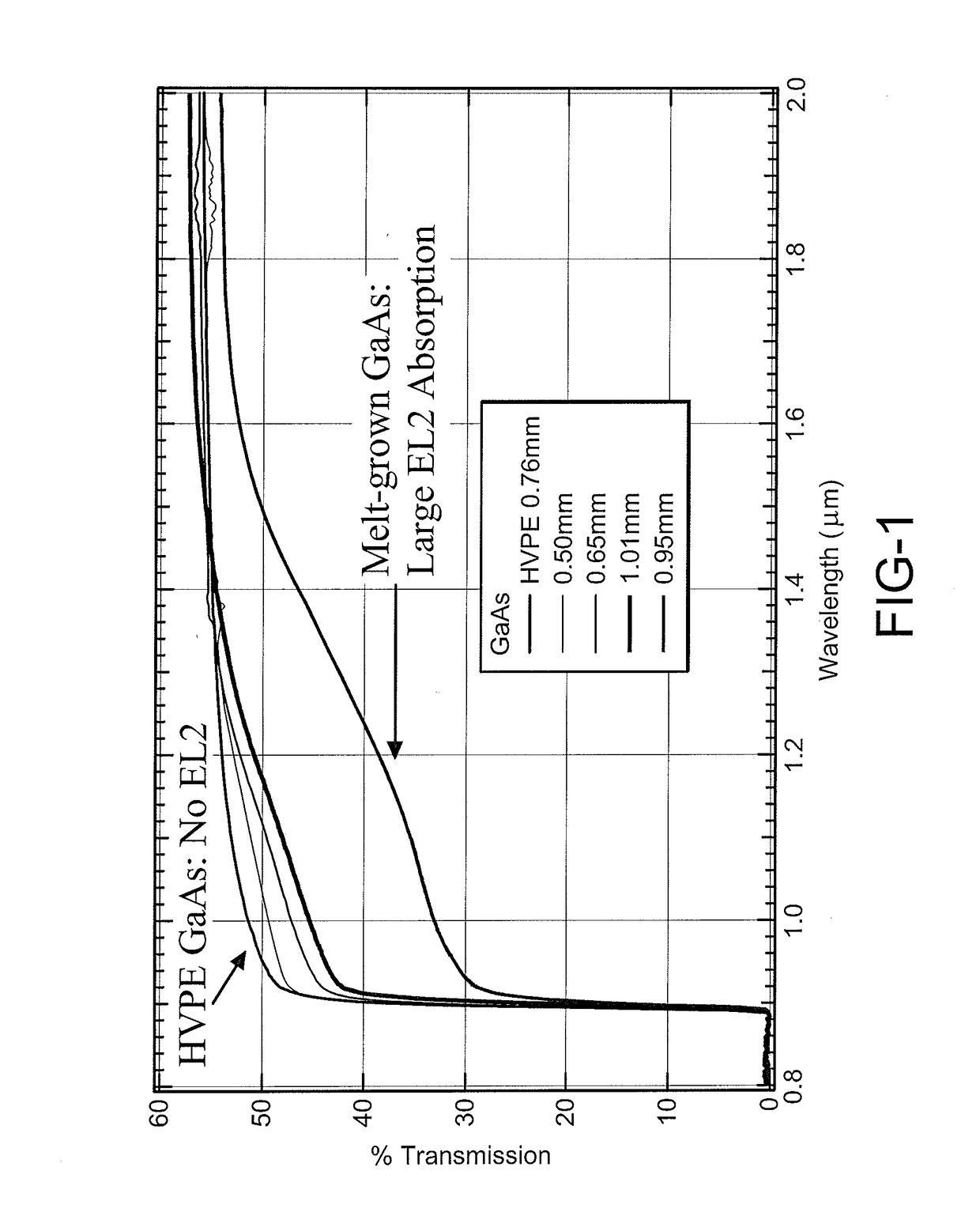
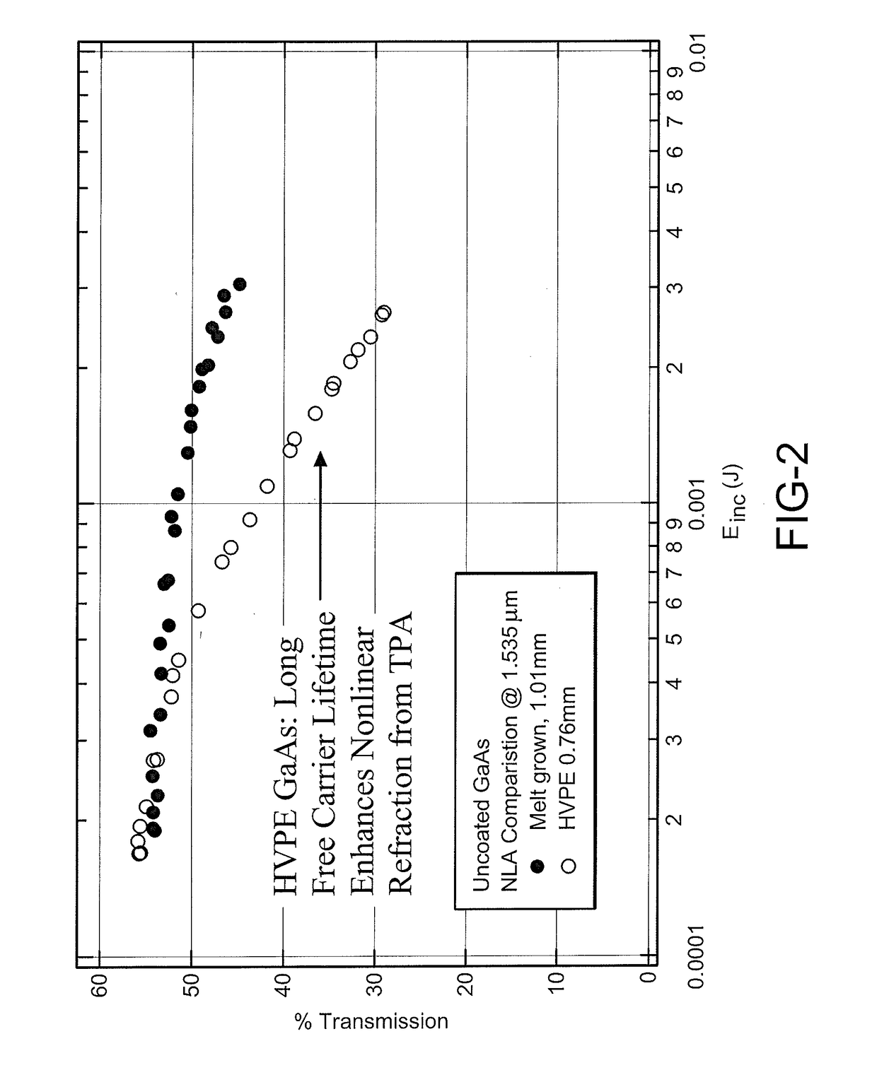
[0030]Data supporting the increased free-carrier lifetime of GaAs grown in the LP-HVPE reactor include optical transmission spectral data, two phot...


PUM

PropertyMeasurementUnit
thicknessaaaaaaaaaa
off-cut angleaaaaaaaaaa

Abstract

A system and method for producing bulk GaAs with an increased carrier lifetime of at least 10 microseconds is provided. The system and method of producing the GaAs crystal involves using a technique called low pressure hydride vapor phase epitaxy (LP-HVPE). In this technique, a gas containing Ga (typically GaCl) is reacted with a gas containing As (typically AsH3) at the surface of a GaAs substrate. When grown under the proper conditions, the epitaxial, vapor grown GaAs crystal has ultra-long free carrier lifetimes of at least one order of magnitude greater than that of the previous lifetime of 1 microsecond. This very long free carrier lifetime GaAs will be particularly useful as a semiconductor radiation detector material and is also expected to be useful for many other applications than include medical imaging, solar cells, diode lasers, and optical limiters and other applications.

Description

CROSS REFERENCE TO RELATED APPLICATION[0001]This application is a continuation-in-part of application Ser. No. 14 / 422,850, filed Feb. 20, 2015, which is a national phase application of PCT Application No. PCT / US2014 / 041932, filed on Jun. 11, 2014, which claims the benefit of U.S. Provisional Application 61 / 833,582, filed on Jun. 11, 2013; the entirety of each is hereby incorporated by reference as if fully rewritten.BACKGROUND[0002]Technical Field[0003]The current disclosure relates generally to a new embodiment of bulk GaAs with an increased carrier lifetime of at least 10 microseconds to be used for optical and electrical devices. The current disclosure also relates to the apparatus, systems, and methods for creating GaAs with very long free carrier lifetimes. More particularly, this very long free carrier lifetime GaAs is expected to be useful as a semiconductor radiation detector material, and also is expected to be useful for applications including, but not limited to, medical ...

Claims


Application Information

Patent Timeline
Patent Type & Authority Applications(United States)
IPC IPC(8): C30B25/14C30B25/12C30B29/42H01L31/0304
CPCC30B25/14C30B29/42C30B25/12H01L31/0304Y02E10/544
Inventor SCHUNEMANN, PETER G.ZAWILSKI, KEVIN T.
Owner BAE SYST INFORMATION & ELECTRONICS SYST INTERGRATION INC
Why Eureka
Try Eureka