

Method of manufacturing diamond, diamond, diamond composite substrate, diamond joined substrate, and tool
- Summary
- Abstract
- Description
- Claims
- Application Information
AI Technical Summary
Benefits of technology
Problems solved by technology
Method used
Image

Examples
first embodiment
Method of Manufacturing Diamond
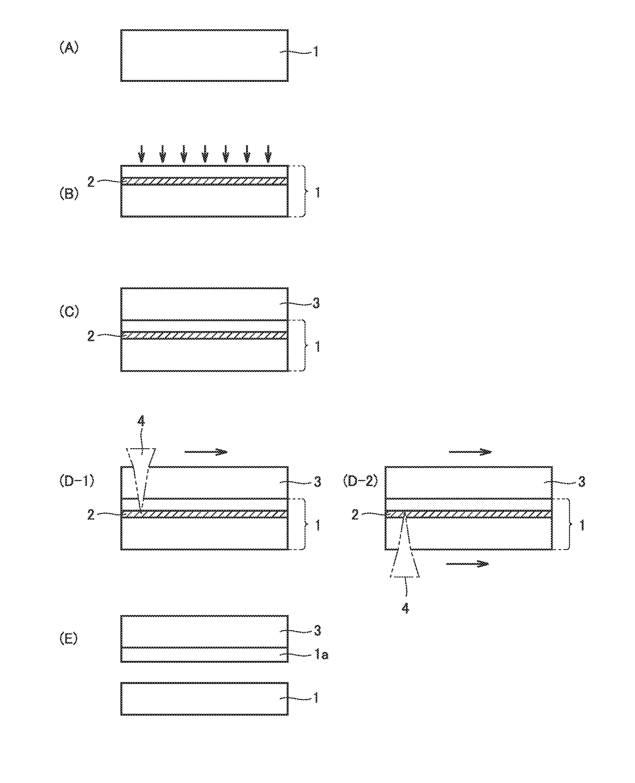
[0076]FIG. 1 (A) to FIG. 1 (E) are diagrams schematically illustrating a method of manufacturing a diamond in an embodiment of the present invention. The method of manufacturing a diamond in the embodiment of the present invention is a method of manufacturing a diamond by a vapor phase synthesis method, and includes the steps of: preparing a substrate 1 including a diamond seed crystal (FIG. 1 (A)); forming, at a predetermined depth from a main surface of substrate 1, a light absorbing layer 2 which is lower in optical transparency than substrate 1, by performing ion implantation into substrate 1 (FIG. 1 (B)); growing a diamond layer 3 on the main surface of substrate 1 by the vapor phase synthesis method (FIG. 1(C)); and separating diamond layer 3 from substrate 1 (FIG. 1 (E)) by applying light from a main surface of at least one of diamond layer 3 and substrate 1 (FIG. 1 (D-1), FIG. 1 (D-2)), to allow light absorbing layer 2 to absorb the light and c...
second embodiment
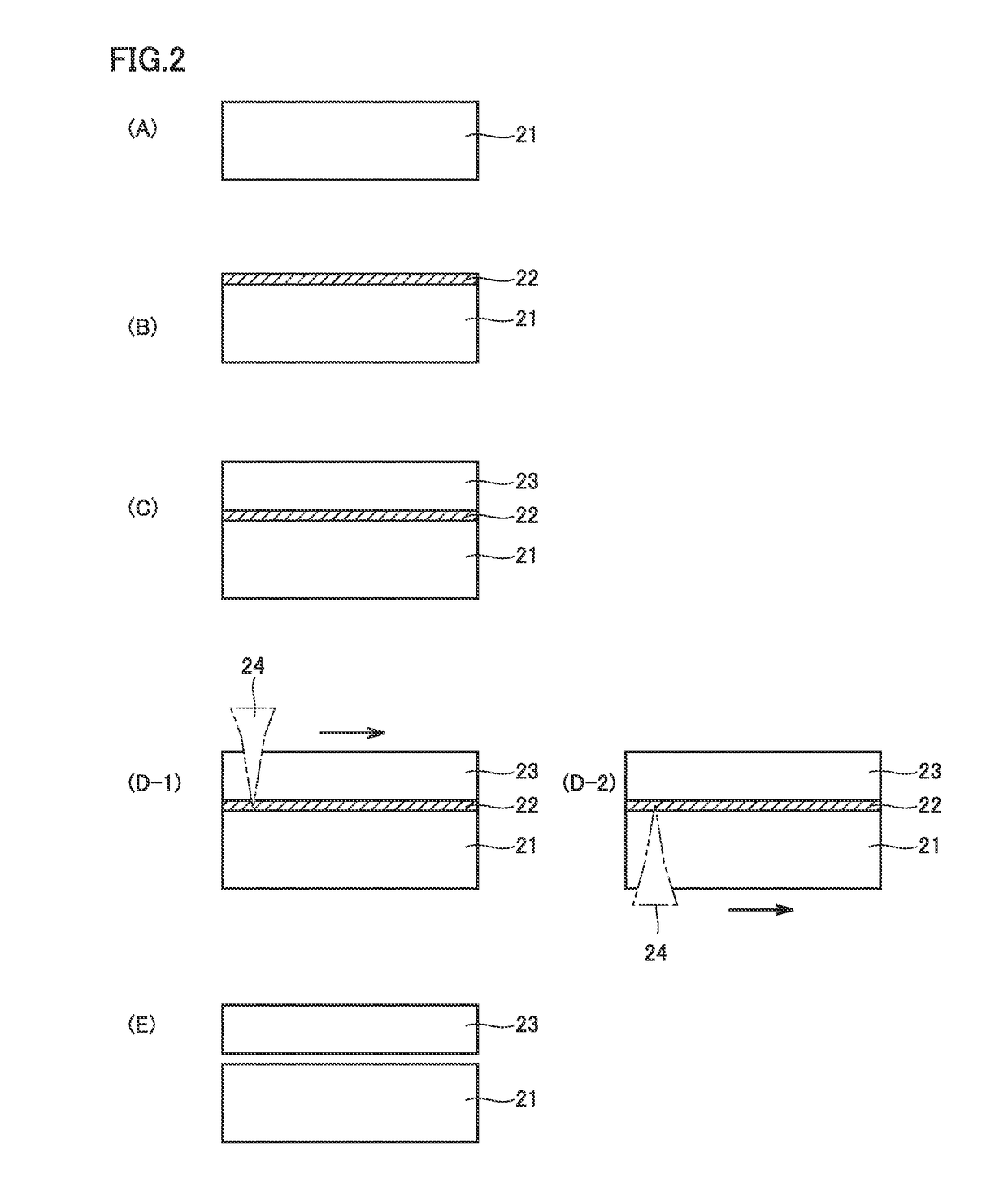
[0122]FIG. 2 (A) to FIG. 2 (E) are diagrams schematically illustrating a method of manufacturing a diamond in an embodiment of the present invention. The method of manufacturing a diamond in the embodiment of the present invention is a method of manufacturing a diamond by a vapor phase synthesis method, and includes the steps of: preparing a substrate 21 including a diamond seed crystal (FIG. 2 (A)); forming a light absorbing layer 22 on a main surface of substrate 21 by the vapor phase synthesis method, the light absorbing layer being lower in optical transparency than substrate 21, having a maximum peak value of a density of atomic vacancies in a range of not less than 0.01% and not more than 20% or having a total atomic concentration of not less than 0.1 ppm and not more than 10% of carbon atoms and different-kind atoms which do not bond with carbon forming a diamond lattice (FIG. 2 (B)); growing a diamond layer 23 on a main surface of light absorbing layer 22 by the vapor phase ...
third embodiment
[0132]A diamond in an embodiment of the present invention is a diamond including: a diamond layer; and a light absorbing layer disposed on one surface of the diamond layer and different in optical transparency from the diamond layer, and a surface of the light absorbing layer includes at least one of a diamond crack having a length of not more than 100 μm, a graphite layer having a maximum diameter of not more than 100 μm, and a graphite layer having a length of not less than 200 μm. The light absorbing layer refers to a layer of not less than 5 nm. The graphite layer may not necessarily be a crystalline layer of graphite, and refers broadly to a graphite layer having a peak called G band appearing at around a Raman shift of 1500 to 1600 cm−1 given by the Raman spectroscopy. The graphite layer having a length of not less than 200 μm refers to a graphite layer which is formed continuously and in which a straight line of 200 μm can be drawn. As to the diamond, when the surface of the ...
PUM
| Property | Measurement | Unit |
|---|---|---|
| Fraction | aaaaa | aaaaa |
| Fraction | aaaaa | aaaaa |
| Fraction | aaaaa | aaaaa |
Abstract
Description
Claims
Application Information