Semiconductor device, manufacturing method thereof, display device, and electronic device

a semiconductor film and semiconductor technology, applied in the direction of semiconductor devices, electrical devices, transistors, etc., can solve the problems of adversely affecting the characteristics of transistors, and achieve the effect of improving the reliability of transistors and reducing the conductivity of oxide semiconductor films

Active Publication Date: 2017-08-24
SEMICON ENERGY LAB CO LTD
View PDF1 Cites 23 Cited by
  • Summary
  • Abstract
  • Description
  • Claims
  • Application Information

AI Technical Summary

Benefits of technology

[0010]In view of the foregoing problems, an object of one embodiment of the present invention is to prevent a change in the electrical characteristics of a transistor including an oxide semiconductor film and to improve the reliability of the transistor. Another object of one embodiment of the present invention is to provide a novel semiconductor device. Another object of one embodiment of the present invention is to provide a novel display device.
[0016]Another embodiment of the present invention is a manufacturing method of a semiconductor device provided with a transistor including an oxide semiconductor film. The oxide semiconductor film is formed over a substrate, a gate insulating layer including at least a silicon oxynitride film is formed thereover, and oxygen plasma treatment is performed on the gate insulating layer. After a gate electrode is formed over the gate insulating layer, heat treatment is performed at a temperature higher than or equal to 150° C. and lower than or equal to 450° C. to diffuse oxygen in the gate insulating layer to the oxide semiconductor film and to decrease conductivity of the oxide semiconductor film.
[0018]Another embodiment of the present invention is a manufacturing method of a semiconductor device provided with a transistor including an oxide semiconductor film. The oxide semiconductor film is formed over a substrate, and a gate insulating layer including at least a silicon oxynitride film is formed thereover. An oxide semiconductor is deposited over the gate insulating layer in an atmosphere containing oxygen by a sputtering method, so that a gate electrode is formed while oxygen is added to the gate insulating layer. After that, heat treatment is performed at a temperature higher than or equal to 150° C. and lower than or equal to 450° C. to diffuse oxygen in the gate insulating layer to the oxide semiconductor film and to decrease conductivity of the oxide semiconductor film.
[0019]One embodiment of the present invention can prevent a change in the electrical characteristics of a transistor including an oxide semiconductor film and improve the reliability of the transistor. One embodiment of the present invention can provide a novel semiconductor device. One embodiment of the present invention can provide a novel display device.

Problems solved by technology

In a transistor that uses an oxide semiconductor film in its channel region, oxygen vacancies which might be formed in the oxide semiconductor film adversely affect the transistor characteristics.

Method used


Image

  • Semiconductor device, manufacturing method thereof, display device, and electronic device
  • Semiconductor device, manufacturing method thereof, display device, and electronic device
  • Semiconductor device, manufacturing method thereof, display device, and electronic device

Examples


embodiment 1

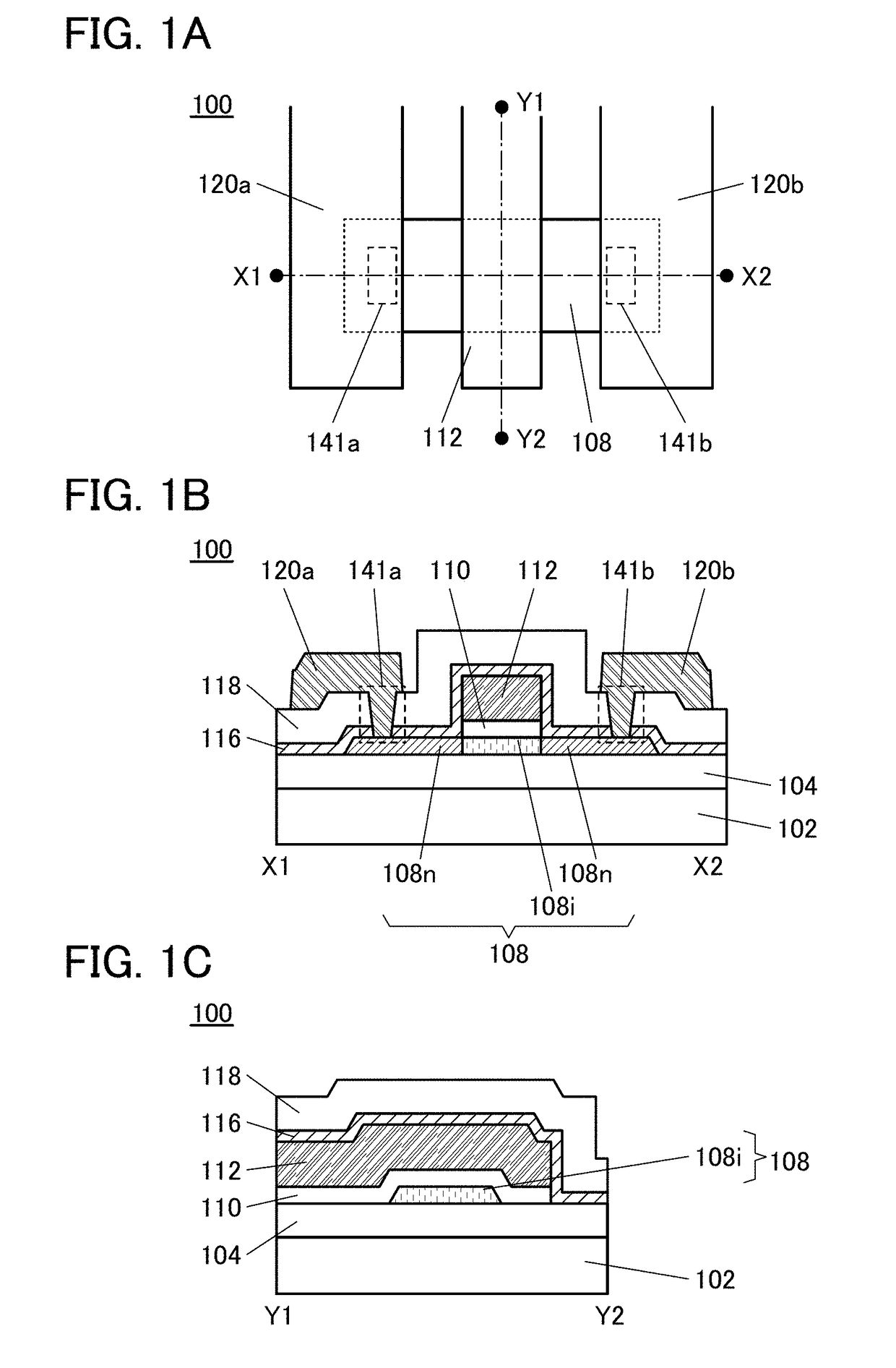
[0094]In this embodiment, a semiconductor device of one embodiment of the present invention that includes a gate insulating film having an excess oxygen region will be described. In addition, a method for manufacturing a semiconductor device of one embodiment of the present invention will be described.

[0095]FIG. 1A is a top view of a transistor 100 of a semiconductor device of one embodiment of the present invention. FIG. 1B is a cross-sectional view taken along a dashed dotted line X1-X2 in FIG. 1A, and FIG. 1C is a cross-sectional view taken along a dashed dotted line Y1-Y2 in FIG. 1A. Note that some components of the transistor 100 (e.g., an insulating film serving as a gate insulating film) are not illustrated in FIG. 1A to avoid complexity. Furthermore, the direction of the dashed dotted line X1-X2 may be referred to as a channel length direction, and the direction of the dashed dotted line Y1-Y2 may be referred to as a channel width direction. As in FIG. 1A, some components ar...

embodiment 2

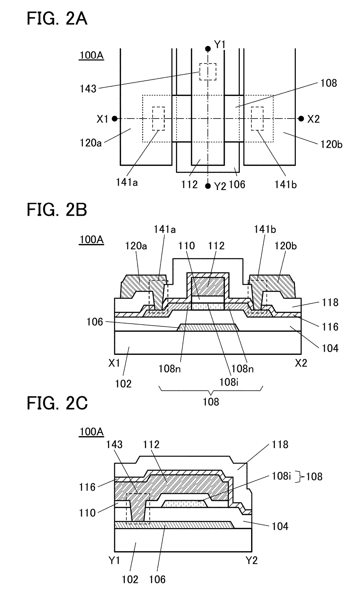
[0287]In this embodiment, a modification example of the transistor described in Embodiment 1 that can be used in one embodiment of the present invention will be described.

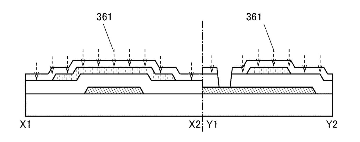
[0288]In the transistor 100C illustrated in FIGS. 4A and 4B, a region 108n2 may be provided between the first region 108i and the second region 108n as illustrated in FIG. 45 in such a manner that the conductive film 112 is formed shorter than the insulating film 110 in the channel length direction of the transistor and heat treatment is performed or an impurity element is added by doping treatment or plasma treatment. The conductivity of the region 108n_2 is higher than that of the first region 108i and lower than that of the second region 108n. The region 108n2 can prevent the intensity of an electric field at an end portion of a drain of the transistor from being increased locally during the operation of a semiconductor device or a display device.

[0289]Note that the structure and method described in this embodim...

embodiment 3

[0290]In this embodiment, an oxide semiconductor that can be used in one embodiment of the present invention will be described.

[0291]An oxide semiconductor preferably contains at least indium or zinc. In particular, indium and zinc are preferably contained. In addition, aluminum, gallium, yttrium, tin, or the like is preferably contained. Furthermore, one or more elements selected from boron, silicon, titanium, iron, nickel, germanium, zirconium, molybdenum, lanthanum, cerium, neodymium, hafnium, tantalum, tungsten, magnesium, and the like may be contained.

[0292]Here, the case where an oxide semiconductor is InMZnO containing indium, an element M, and zinc is considered. The element M is aluminum, gallium, yttrium, tin, or the like. Alternatively, the element M can be boron, silicon, titanium, iron, nickel, germanium, zirconium, molybdenum, lanthanum, cerium, neodymium, hafnium, tantalum, tungsten, magnesium, or the like. Note that two or more of the above elements may be used in co...


PUM


Abstract

The field-effect mobility and reliability of a transistor including an oxide semiconductor film are improved. Provided is a semiconductor device including an oxide semiconductor film. The semiconductor device includes a first insulating film, an oxide semiconductor film over the first insulating film, a second insulating film and a third insulating film over the oxide semiconductor film, and a gate electrode over the second insulating film. The second insulating film comprises a silicon oxynitride film. When excess oxygen is added to the second insulating film by oxygen plasma treatment, oxygen can be efficiently supplied to the oxide semiconductor film.

Description

TECHNICAL FIELD[0001]One embodiment of the present invention relates to a semiconductor device including an oxide semiconductor film, a method for manufacturing the semiconductor device, a display device including the semiconductor device, and an electronic device including the semiconductor device.[0002]Note that one embodiment of the present invention is not limited to the above technical field. The technical field of one embodiment of the invention disclosed in this specification and the like relates to an object, a method, or a manufacturing method. In addition, one embodiment of the present invention relates to a process, a machine, manufacture, or a composition of matter. In particular, one embodiment of the present invention relates to a semiconductor device, a display device, a light-emitting device, a power storage device, or a memory device, or a driving method or manufacturing method thereof.[0003]In this specification and the like, a semiconductor device generally means ...

Claims


Application Information

Patent Timeline
Patent Type & Authority Applications(United States)
IPC IPC(8): H01L21/385H01L21/44H01L21/4757H01L21/443H01L29/66H01L21/02H01L29/49H01L29/786H01L29/04
CPCH01L21/385H01L29/7869H01L21/44H01L21/4757H01L29/045H01L29/66969H01L29/518H01L21/02274H01L21/02326H01L29/4908H01L21/443H01L29/78648H01L21/0214H01L27/1225H01L21/0217H01L21/022H01L21/02323H01L21/0234
Inventor JINTYOU, MASAMIKOEZUKA, JUNICHIHAMOCHI, TAKASHIHOSAKA, YASUHARU
Owner SEMICON ENERGY LAB CO LTD
Why Eureka
Try Eureka