

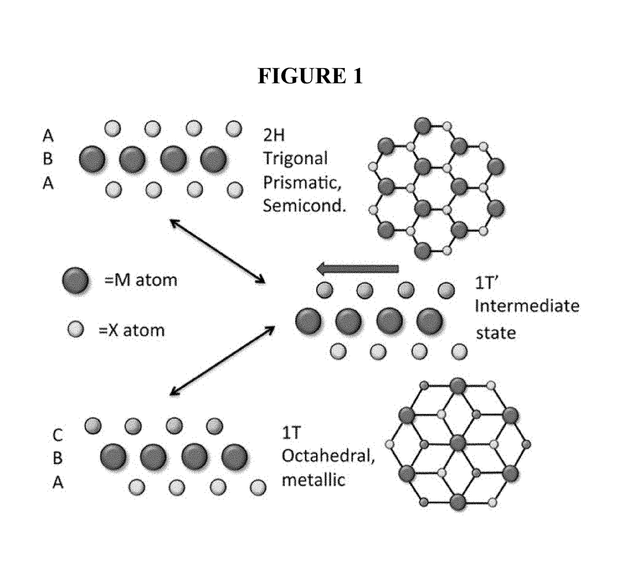
2h to 1t phase based transition metal dichalcogenide sensor for optical and electronic detection of strong electron donor chemical vapors
a technology of transition metal dichalcogenide and chemical vapor, which is applied in the direction of fluorescence/phosphorescence, instruments, and material electrochemical variables, can solve the problems of partial reduction of pl, difficult measurement, and difficult tem study of most commonly studied high-quality mechanically exfoliated films, and achieve high-precision detection.
- Summary
- Abstract
- Description
- Claims
- Application Information
AI Technical Summary
Benefits of technology
Problems solved by technology
Method used
Image


Examples
example 1
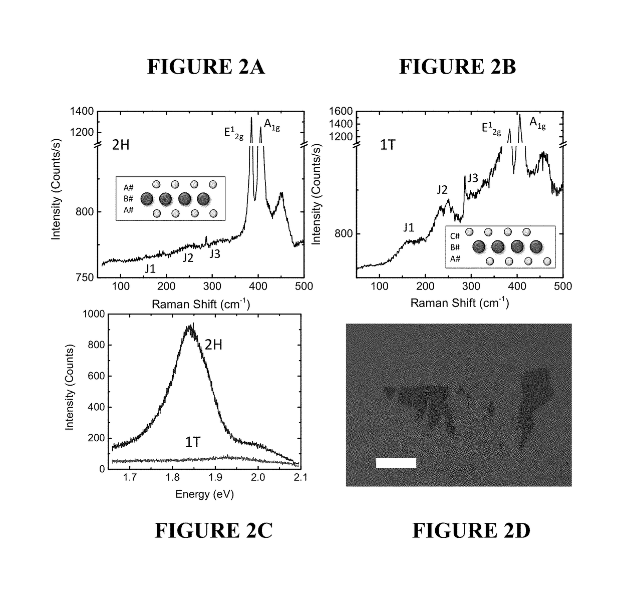
[0099]MoS2 flakes were mechanically exfoliated from a bulk crystal onto 275 nm SiO2 / n+ Si. Thin layers were first visually identified with an optical microscope and then confirmed to be monolayer through Raman spectroscopy, as shown in FIGS. 2A and 2B, and photoluminescence spectroscopy (PL), shown in FIG. 2C. For Raman spectroscopy, the peak-to-peak separation of the E12g and A1g modes was associated with the number of layers, with a distance of ˜18 cm−1 being attributed monolayers and ˜21.5 cm−1 for bilayers (C. Lee, et al., “Anomalous lattice vibrations of single- and few-layer MoS2,” ACS Nano 4:2695 (2010)). For PL, because of the direct-to-indirect bandgap transition, a strong emission peak due to the A-exciton dominates for monolayers (A. Splendiani, et al., “Emerging photoluminescence in monolayer MoS2,” Nano Lett. 10:1271-1275 (2010)). As the number of layers increases, the intensity of the peak decreases rapidly and the position shifts to lower energy because of the drastic...
example 2
[0102]After the identification of MoS2 flakes suitable for optical-based chemical vapor sensing, before-exposure PL and Raman scans were obtained, shown for a typical sample in FIGS. 3A and 3B, respectively. The films were then exposed to a strong electron donor vapor (in this case, tripropyl amine, or TPA). After exposure, the PL and Raman scans were re-taken, as shown in FIGS. 3A and 3B. The PL and Raman spectra of the material can be compared after exposure to the 1T state scans taken in FIG. 2B. A sharp decrease in PL intensity was observed, indicative of the 1T state. The appearance of the Raman J1, J2, and J2 peaks was observed, coupled with a wider E12g peak, also indicative of the 1T state. Therefore, it could be concluded that the MoS2 film had at least partially transitioned to the 1T state due to exposure to a strong electron donor vapor. For sensor applications, a film can be exposed to an unknown analyte. If the PL and Raman after exposure indicates a phase change, then...
example 3
[0104]The film formed in Example 2 was exposed to the strong electron donor triethylamine (TEA) while passing a voltage through the sample and monitoring the device's resistance. FIG. 4A is an optical image of a completed MoS2 FET sensor device, showing electrical evidence of a chemical vapor induced phase change, where the scale bar is 5 μm. In the beginning, the sample showed a response to pulses of analyte, as shown in the top line of FIG. 4B and discussed in the literature (F. K. Perkins, et al., “Chemical vapor sensing with monolayer MoS2,” Nano Lett. 13:668-673 (2013); and A. L. Friedman, et al., “Chemical vapor sensing to two-dimensional MoS2 field effect transistor devices,”Sol. St. Elec. 101:2-7 (2014)). FIG. 4B is a graph plotting resistance vs. time for the three stages of sensing: (1) The device responds (middle line) to the pulsed strong electron donor triethyl amine (TEA) and is in the 2H semiconducting phase. The peaks are the peaks of the pulses. (2) However, after a...
PUM
| Property | Measurement | Unit |
|---|---|---|
| Time | aaaaa | aaaaa |
| Magnetic field | aaaaa | aaaaa |
| Power | aaaaa | aaaaa |
Abstract
Description
Claims
Application Information