Method of manufacturing graphene using metal catalyst
a metal catalyst and graphene technology, applied in the direction of catalyst activation/preparation, metal/metal-oxide/metal-hydroxide catalyst, physical/chemical process catalyst, etc., can solve the problem of not being able to easily grow epitaxial graphene layers, multilayer graphene is present as islands, and barely acting as catalysts
- Summary
- Abstract
- Description
- Claims
- Application Information
AI Technical Summary
Benefits of technology
Problems solved by technology
Method used
Image
Examples
example 1
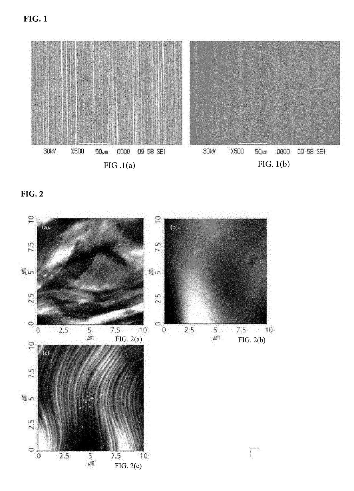
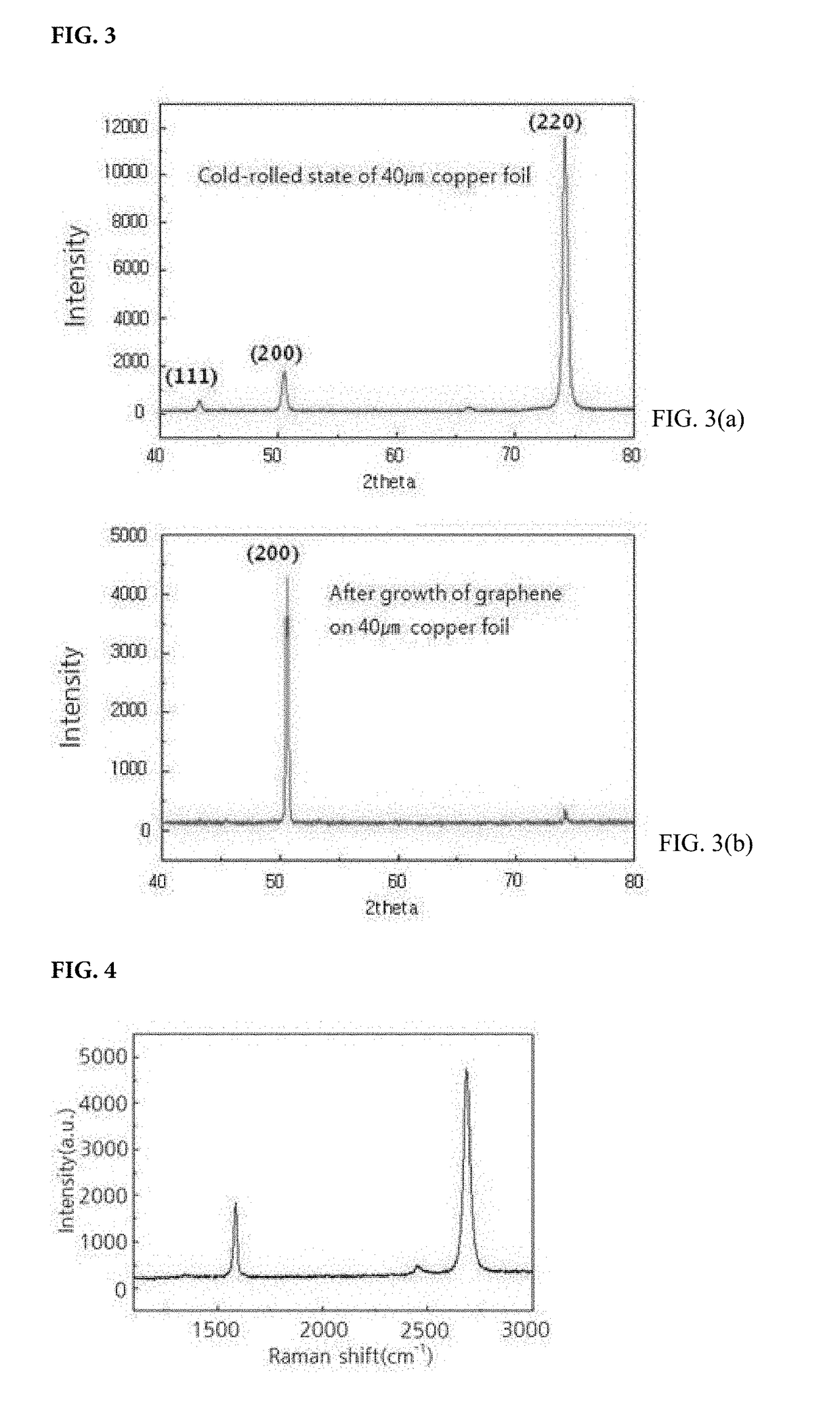
[0040]Fabrication of graphene thin film on rolled copper foil Tough pitch copper foils (a purity of 99.9% or more, an oxygen content of 0.05% or less) having thicknesses of 0.5 mm and 0.2 mm were annealed, and then cold-rolled to thicknesses of 12 μm, 25 μm, 40 μm, 50 μm and 100 μm. The cold rolled foils were heated at various annealing temperatures so that 95% or more thereof was oriented in the (100) direction. It was confirmed that a graphene thin film was evenly formed on the annealed foils (see FIG. 1). After recrystallization, only crystal growth occurred on the foils, and thus the orientation of the foils did not change to a new orientation. Table 1 below shows the results of forming graphene layer at various reduction ratios under various heat treatment conditions.
TABLE 1ThicknessThicknessFormationof rawafter(100)Recrystallization ofmaterialrollingReductionplaneannealingmonolayer(mm)(μm)ratio (%)orientation temperature (° C.)graphenePreparation0.21294◯200◯Example 1Preparatio...
example 2
Fabrication of Graphene Layer on Electrodeposited Copper Plated Tough Pitch Copper Foil
[0044]2-1: Fabrication of Electrodeposited Copper Foil by Pulse-Current Plating and Graphene Layer
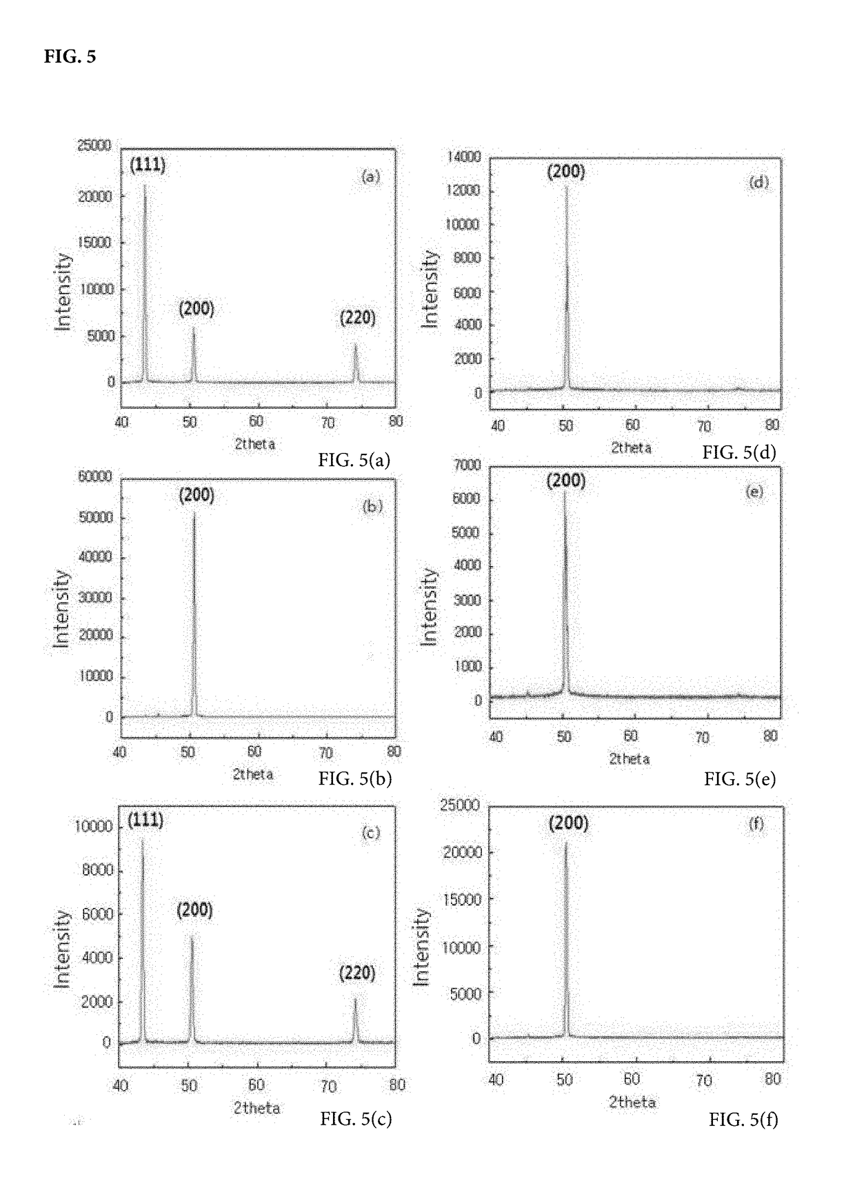
[0045]Plain tough pitch copper foils were air-stirred in a solution composed of 180-330 g / L of copper sulfate pentahydride (CuSO4.5H2O), 40-120 g / L of sulfuric acid and 40-120 ppm of hydrochloric acid at a temperature of 30˜55° C. and a current density of 1-10 A / dm2, thereby pulse current plating the foils. The results are shown in FIG. 5, and the pulse waveform is expressed as current supply time: rest time.
[0046]FIGS. 5(a) and 5(b) show the results of measuring the state of a specimen obtained by plating copper on a copper foil at a ratio of 80:20 at a current density of 4.2-4.3 A / dm2 and the orientation of a structure obtained by growing graphene on the specimen at 1000° C.; FIGS. 5(c) and 5(d) show the results of measuring the state of a specimen obtained by plating copper on a copper foil at a ra...
example 3
Formation of Graphene on Copper Alloy Catalyst Substrate
[0053]A copper alloy foil containing 140 ppm of silver (see FIG. 9(b)) was heated at 600° C. for 30 minutes in an atmosphere of 70 sccm methane and 10 sccm hydrogen, and whether graphene was formed on the alloy foil was examined. As a control, copper (see FIG. 9(a)) was treated under the same conditions, and whether graphene was formed thereon was examined (see FIG. 9).
[0054]It can be seen that, when graphene was formed on copper, graphene islands and carbides were formed, but on the silver-containing copper alloy, graphene was epitaxially formed. However, when copper was previously annealed at 800° C. to form steps, graphene was epitaxially formed thereon.
[0055]The above copper alloy and copper had a hexagonal lattice structures having the (111) or (100) orientation after annealing, and these catalyst substrates also had the same orientation in the following examples.
[0056]Thus, it could be seen that the addition of a substitu...
PUM
| Property | Measurement | Unit |
|---|---|---|
| Temperature | aaaaa | aaaaa |
| Temperature | aaaaa | aaaaa |
| Fraction | aaaaa | aaaaa |
Abstract
Description
Claims
Application Information


