
Self-powered ghz solution-processed hybrid perovskite photodetectors

a photodetector and solution processing technology, applied in the field of photodetector systems, can solve the problems of slowing down the low response speed of the solution-processed photodetectors, and little information about the operation speed of the oihp photodetectors, so as to improve the response speed, fast response speed, and charge trap

Active Publication Date: 2018-03-15
NUTECH VENTURES
View PDF2 Cites 16 Cited by
  • Summary
  • Abstract
  • Description
  • Claims
  • Application Information

AI Technical Summary

Benefits of technology

The patent provides a way to make photodetectors that can respond quickly to high-speed processes, such as the decay of fluorescence materials. By using a special material called OIHP, the devices can operate at very high frequencies without needing to be powered. The technique eliminates charge trapping and removes limitations caused by resistance and capacitance, resulting in devices that can measure things in real-time.

Problems solved by technology

These devices heavily rely on traditional inorganic semiconductor materials such as silicon, indium gallium arsenide, gallium nitride, et al, which are generally deposited by expensive, slow, high temperature processes such as molecular beam epitaxy (MBE) and metal-organic chemical vapor deposition (MOCVD).
Nevertheless, despite of the significant progress in these aspects, one challenge to be addressed is the low response speed of the solution-processed photodetectors.
In addition, the presence of charge traps in many of these solution-processed semiconductors, sometimes intentionally introduced to generate a photoconductive gain, inevitably slow-down their response speed.
Despite the rapid progress in sensitivity enhancement of perovskite photodetectors, however, little is known about how fast the OIHP photodetectors can operate.
Despite of the high sensitivity demonstrated, the response speeds of solution-processed photodetectors are generally low due to the low carrier mobility and the long charge traps of most solution-processed semiconductors.

Method used


Image

  • Self-powered ghz solution-processed hybrid perovskite photodetectors
  • Self-powered ghz solution-processed hybrid perovskite photodetectors
  • Self-powered ghz solution-processed hybrid perovskite photodetectors

Examples


examples

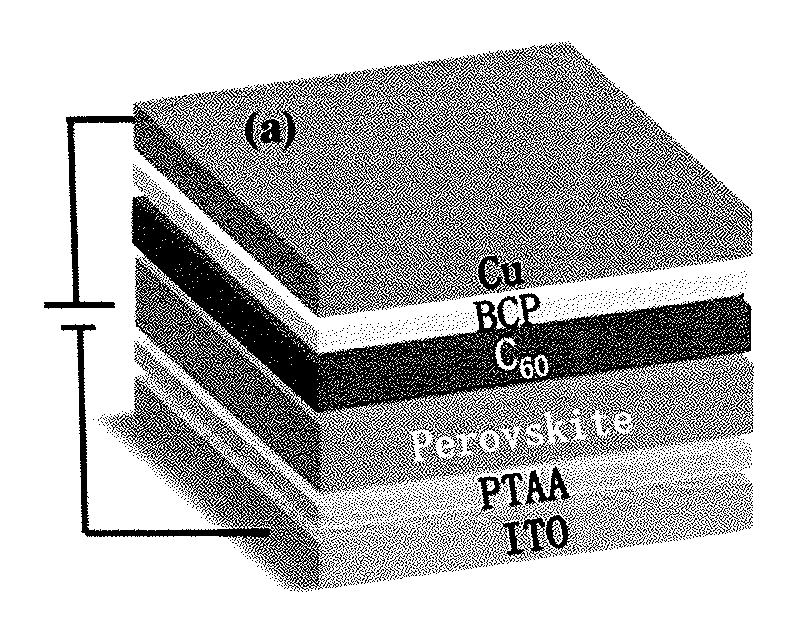
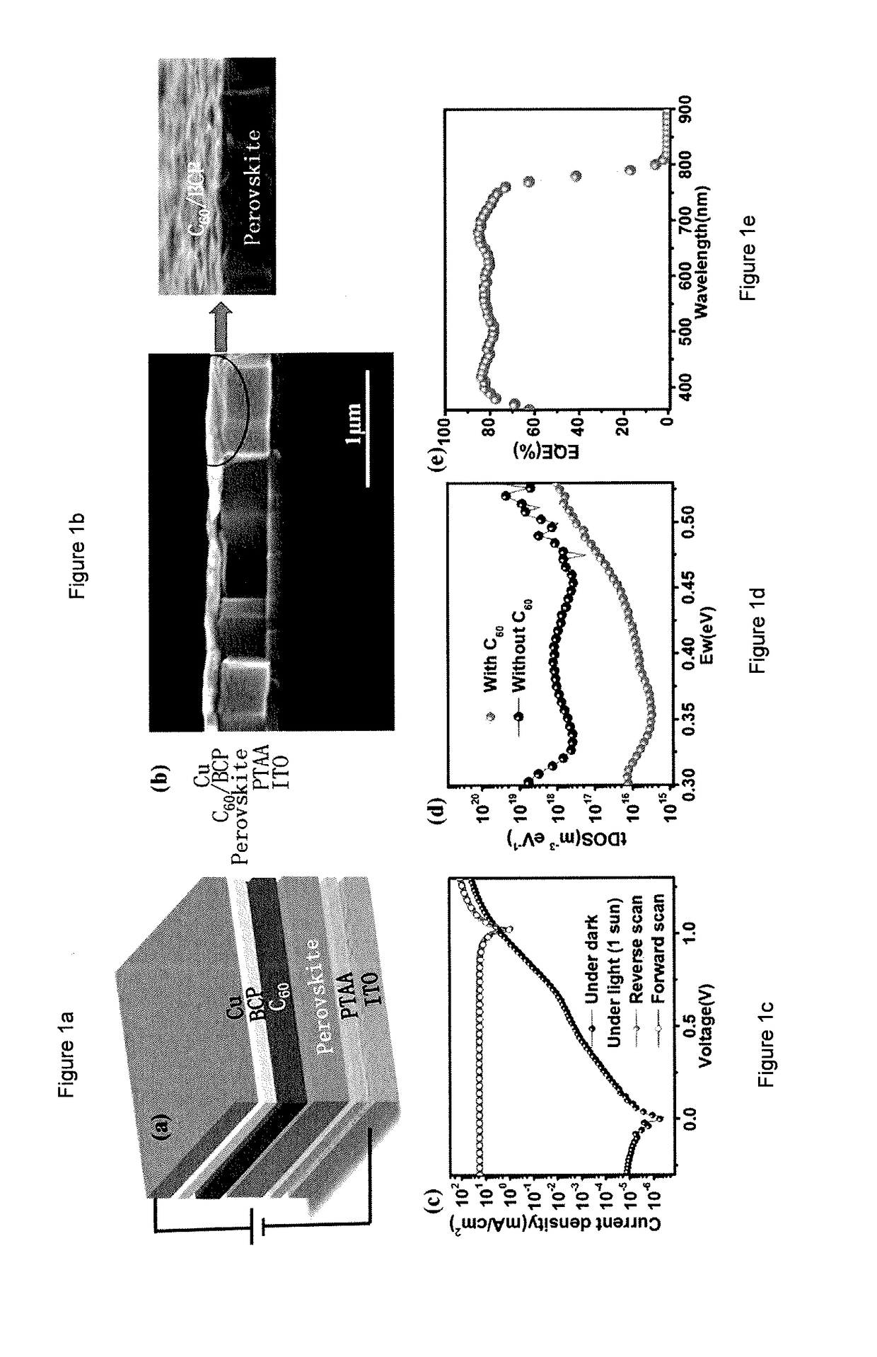
[0049]Device fabrication. PTAA dissolved in toluene was spun on clean ITO substrates at a speed of 5,000 rounds per minute (rpm). The film was then annealed at 100° C. for 10 min. PbI2 and MAI were dissolved in dimethylformamide (DMF) and 2-propanol with concentrations of 630 mg ml−1 and 65 mg ml−1, respectively. The PbI2 solution was spun on a PTAA layer at 6,000 rpm for 35 s. Then the PbI2 film was transferred onto a hot plate at 90° C. for quick drying. Afterwards, the MAI solution was spun on top of the PbI2 film at 6,000 rpm for 35 s at room temperature, combined with a thermally annealing at 100° C. for 1 h. Finally, the device was completed by thermal evaporating C60 (30 nm), BCP (8 nm) and Cu (80 nm) in sequential order.

[0050]Device characterization.

[0051]AM 1.5G simulated irradiation with an intensity of 100 mW cm−2 was produced by a Xenon-lamp-based solar simulator (Oriel 67005, 150 W) for Current (I)-voltage (V) measurements. The light intensity was calibrated by a silico...


PUM


Abstract

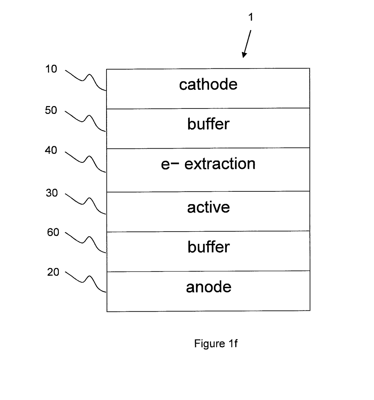
Organic-inorganic hybrid perovskite (OIHP) based photo-responsive devices include an OIHP active layer disposed between a cathode layer and an anode layer, and an electron extraction layer disposed between the cathode layer and the active layer. The electron extraction layer includes a layer of C60 directly disposed on the active layer. The active layer includes an organometal trihalide perovskite layer (e.g., CH3NH3PbI2X, where X includes at least one of Cl, Br, or I).

Description

CROSS-REFERENCE TO RELATED APPLICATIONS[0001]This patent application is a Continuation-in-Part of U.S. Non-provisional Patent Application No. 15 / 009,701, filed Jan. 28, 2016, which claims the benefit of U.S. Provisional Application No. 62 / 108,863, filed Jan. 28, 2015, and is a Continuation-in-Part of U.S. Non-provisional Patent Application No. 14 / 576,878, filed Dec. 19, 2014, (now U.S. Pat. No. 9,391,287), which claims the benefit of U.S. Provisional Patent Application No. 61 / 918,330, filed on Dec. 19, 2013, all of which are incorporated herein by reference. This application also claims the benefit of U.S. Provisional Patent Application No. 62 / 381,412, filed Aug. 30, 2016, which is incorporated herein by reference.FEDERALLY SPONSORED RESEARCH OR DEVELOPMENT[0002]This invention was made with Government support under contract N000141210556 awarded by The Office of Naval Research, and under contract 2014-DN-077-ARI069-02 awarded by The Department of Homeland Security. The Government ha...

Claims


Application Information

Patent Timeline
IPC IPC(8): H01G9/16H01G9/20H01L51/44H01L51/00G01J1/42G01J1/04
CPCH01G9/16H01G9/2009H01L51/448H01L51/0046G01J1/42G01J1/0411H01L51/4213C30B7/06C30B29/54H01L31/076Y02E10/549H01L2031/0344Y02E10/542Y02E10/548H10K30/57H10K85/215H10K30/20H10K85/50H10K30/50H10K85/211H10K30/88H10K30/10H10K30/353
Inventor HUANG, JINSONG
Owner NUTECH VENTURES
Learn More