

Method for producing composite wafer having oxide single-crystal film
- Summary
- Abstract
- Description
- Claims
- Application Information
AI Technical Summary
Benefits of technology
Problems solved by technology
Method used
Image

Examples
experiment 1
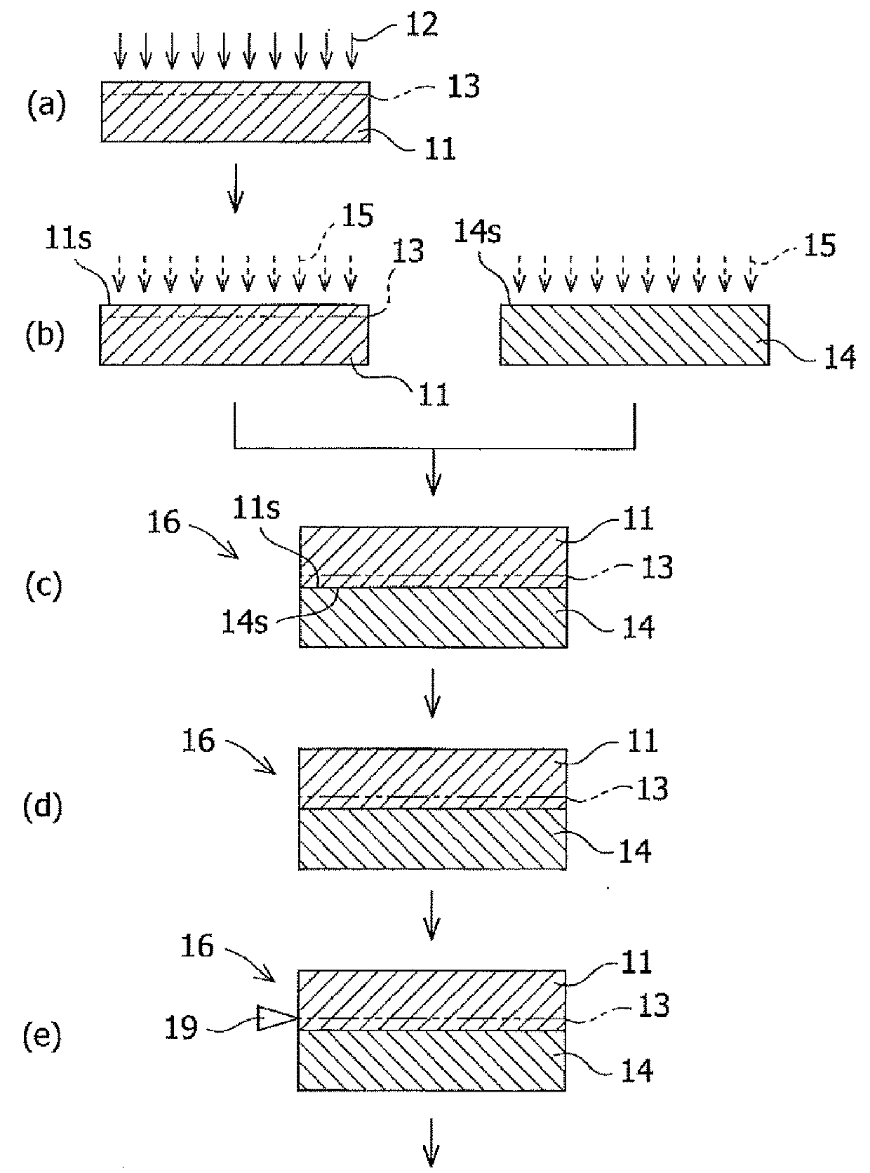
[0048]As a support wafer, a sapphire wafer having a diameter of 100 mm and a thickness of 0.35 mm was used. As an oxide single-crystal wafer, a lithium tantalate wafer having a diameter of 100 mm and a thickness of 0.35 mm was used. The surface roughness RMS of each surface of the sapphire wafer and the lithium tantalate wafer to be bonded together was determined using an atomic force microscope to be 1.0 nm or less.
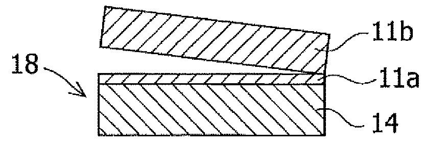
[0049]The respective surfaces of the sapphire wafer and the lithium tantalate wafer to be bonded together were subjected to surface activation by plasma treatment with a plasma activation apparatus in a nitrogen atmosphere. Next, the surface-activated surfaces of the sapphire wafer and the lithium tantalate wafer were bonded together at room temperature (25° C.) to obtain a laminate. Each of the laminates thus obtained was heated to a temperature of 70, 80, 90, 100, 110, 125, 150, 175, 200, 225, 250, or 275° C. and heat-treated at the temperature for 24 hours. A heat tre...
experiment 2
[0050]Laminates were obtained and heat-treated in the same manner as in Experiment 1 except that a silicon wafer having a diameter of 100 mm and a thickness of 0.35 mm was used as the support wafer, and each laminate thus obtained was heated to a temperature of 70, 80, 90, 100, 110, 125, 150, 175, 200, or 225° C. and heat-treated at the temperature for 24 hours. Each of the surface of the silicon wafer and the surface of the lithium tantalate wafer to be bonded together had a surface roughness RMS of 1.0 nm or less. The result of the appearance inspection of each laminate thus obtained is shown in Table 1. It is confirmed that the laminate samples obtained using a silicon wafer as the support wafer and the heat treatment at 0 to 200° C. had neither cracking nor chipping.
experiment 3
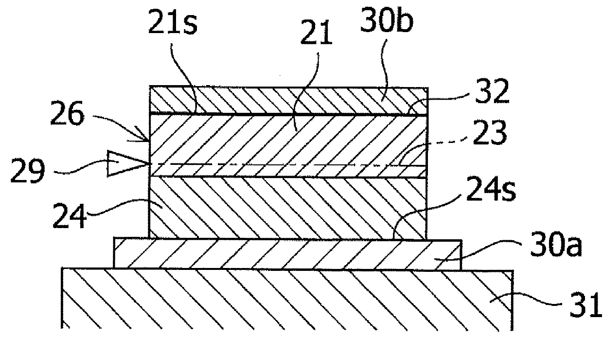
[0051]Laminates were obtained and heat-treated in the same manner as in Experiment 1 except that a silicon wafer with an oxide film containing a silicon wafer having a diameter of 100 mm and a thickness of 0.35 mm and a 100-nm oxide film on the silicon wafer was used as the support wafer, and each laminate thus obtained was heated to a temperature of 70, 80, 90, 100, 110, 125, 150, 175, 200, or 225° C., and heat-treated at the temperature for 24 hours. Each of the surface of the silicon wafer with an oxide film and the surface of the lithium tantalate wafer to be bonded together had a surface roughness RMS of 1.0 nm or less. The result of the appearance inspection of each laminate thus obtained is shown in Table 1. The silicon wafer with an oxide film was obtained by heat-treating a silicon wafer at 1100° C. for about one hour to allow a 100-nm thermal oxide film to grow on the silicon wafer. It is confirmed that the laminate samples obtained using the silicon wafer with an oxide fi...
PUM
 Abstract
Description
Claims
Application Information