Additive manufacturing processes and additively manufactured products

a technology of additive manufacturing and manufacturing process, applied in the direction of manufacturing tools, semiconductor/solid-state device details, lighting and heating apparatus, etc., can solve the problems of device failure, interconnection breakage, and inability to directly integrate these novel additive manufacturing devices directly onto electronic devices, so as to minimize thermal stress, improve bonding, and improve bonding strength

Active Publication Date: 2020-02-13
THE RES FOUND OF STATE UNIV OF NEW YORK
View PDF0 Cites 19 Cited by
  • Summary
  • Abstract
  • Description
  • Claims
  • Application Information

AI Technical Summary

Benefits of technology

[0029]Embodiments may include using one or more of these active elements plus a solder. Embodiments may also include solders that mix elements such as Sn, Pb, Ag, Cu, Sb, Bi, In, Zn, Cd, Au, Ni, Si, Ge, Si, Al. Embodiments includes solders such as InSn (e.g., In52Sn48, In60Sn40, In50Sn50, In42Sn58), InCd (e.g., In74Cd26), BiPbInCdSn (e.g., Bi44.7Pb22.6In19.1Cd5.3Sn8.3), InBiSn (e.g., In51Bi32.5Sn16.5), InBiCd (e.g., In61.7Bi30.8Cd7.5), BiPbSnIn (e.g., Bi49Pb18Sn12In21), BiPbSnCd (e.g., Bi50Pb26.7Sn13.3Cd10), BiSnIn (e.g., Bi56Sn30In14), BiPbSn (e.g., Bi52Pb32Sn16, Bi50Pb31.2Sn18.8), BiPb (e.g., Bi58Pb42), SnPbBi (e.g., Sn46Pb46Bi8), InSnPbCd (e.g., In70Sn15Pb9.6Cd5.4), SnPbIn (e.g., Sn54Pb26In20, Sn37.5Pb37.5In25, Sn70Pb18In12), BiSnAg (e.g., Bi57Sn42Ag1), BiSn (e.g., Bi56Sn42, Bi58Sn42), SnBiPb (e.g., Sn48Bi32Pb20, Sn43Pb43Bi14), CdSn (e.g., Cd70Sn30), InPbAg (e.g., In80Pb15Ag5), InAg (e.g., In97Ag3, In90Ag10), SnPbCd (e.g., Sn51.2Pb30.6Cd18.2), InPb (e.g., In75Pb25, In70Pb30, In60Pb40, In50Pb50, Pb75In25), In, PbSnZn (e.g., Pb63Sn34Zn3), SnZnInBi (e.g., Sn86.5Zn5.5In4.5Bi3.5), SnInAg (e.g., Sn77.2In20Ag2.8, Sn86.9In10Ag3.1, Sn91.8In4.8Ag3.4, Sn88In8.0Ag3.5Bi0.5), SnZnCd (e.g., Sn40Zn27Cd33), SnPbZn (e.g., Sn30Pb50Zn20), PbSnAg (e.g., Pb54Sn45Ag1, Sn62Pb36Ag2, Pb80Sn18Ag2, Pb96Sn2Ag2, Pb88Sn10Ag2, Pb92Sn5.5Ag2.5, Pb90Sn5Ag5, Pb93.5Sn5Ag1.5, Pb95.5Sn2Ag2.5), SnZnIn (e.g., Sn83.6Zn7.6In8.8), PbSn (e.g., Pb90Sn10, Pb85Sn15, Pb80Sn20, Sn63Pb37, Sn70Pb30, Sn90Pb10, Sn63Pb37P0.0015-0.04, Sn62Pb37Cu1, Sn97.5Pb1Ag1.5,), SnZnBi (e.g., Sn89Zn8Bi3), SnZn (e.g., Sn91Zn9, Sn85Zn15, Sn60Zn40, Zn70sn30, Zn60Sn40, Sn50Zn49Cu1, Sn90Zn7Cu3), SnBiAg (e.g., Sn91.8Bi4.8Ag3.4), SnAgCu (e.g., Sn96.5Ag3.0Cu0.5, Sn95.5Ag4.0Cu0.5, Sn95.8Ag3.5Cu0.7, Sn95.6Ag3.5Cu0.9, Sn99Cu0.7Ag0.3, Sn96.2Ag2.5Cu0.8Sb0.5, Sn90.7Ag3.6Cu0.7Cr5, Sn95Ag3.5Zn1Cu0.5, Sn95.5Cu4Ag0.5, Sn97Cu2.75Ag0.25), SnAu (e.g., Sn90Au10), SnAg (e.g., Sn96.5Ag3.5—Sn93Ag7), SnCu (e.g., Sn99.3Cu0.7, Sn97Cu3), SnPbZn (e.g., Sn33Pb40Zn28), Sn, SnSb (e.g., Sn95Sb5—Sn99Sb1), SnAgSb (e.g., Sn64Ag25Sb10), PbIn (e.g., Pb81In19, Pb70In30, Pb75In25, Pb90In5Ag5, Pb92.5In5Ag2.5, Pb92.5In5Au2.5), CdZn (e.g., Cd82.5Zn17.5, Cd70Zn30, Cd60Zn40, Zn90Cd10, Zn60Cd40, Cd78Zn17Ag5), Bi, AuSn (e.g., Au80Sn20), PbSbSn (e.g., Pb80Sb15Sn5), PbAg (e.g., Pb94.5Ag5.5—Pb96Ag4, Pb97Ag1.5Sn1, Pb97.5Ag2.5), CdAg (e.g., Cd95Ag5), AuSi (e.g., Au98Si2, Au96.8Si13.2), ZnAl (e.g., Zn95Al5), ZnSn (e.g., Zn95Sn5), Zn, AuIn (e.g., Au82In18), AuGe (e.g., Au87.5Ge12.5). Many of these possible bonding alloys are undesirable for due to health and environmental concerns (e.g., those containing Pb, Cd), and for economics due to cost (e.g., Au). However, these are not technologically excluded, and may be employed as appropriate in the application. Aluminum containing solders have advantage for bonding to Al2O3-based substrates.
[0030]In another embodiment, the bonding metal is a homogeneous or heterogeneous powder mixture of a brazing alloy. One specific embodiment of this invention uses the Sn3Ag4Ti composition as a heterogeneous or homogeneous composed powder. This alloy has good bonding strength with dissimilar metallic or non-metallic substrates at temperatures between 250° C. to 450° C. [15, 59, 17, 18]. Sn3Ag4Ti forms bonds with such materials as oxides (e.g., silica glass, quartz, borosilicate glass, alumina, beryllia, ceria, zirconia, lithium aluminum silicates, gallium oxide, indium tin oxide, indium zinc oxide), silicides (e.g., molybdenum disilicide), nitrides, and carbides, carbon materials (e.g., diamond, pyrolytic graphite, carbon nanotubes, graphene, fullerenes), borides (e.g., tungsten borides), arsenides (e.g., gallium arsenide), sulfides (e.g., zinc sulfide). To form a good bond, the braze or bonding alloy must minimize thermal stress from the solidification temperature to ambient, so the low melting point of the braze is beneficial. Furthermore, the low melting point increases the activity of the reactive metals by making it more available to react with the substrate. Brazing alloys generally have similar compositions to low-temperature solders, but also include an element that thermodynamically favors forming reactions with the substrate over other elements of the solder. Unlike a solid solution alloy with the different species randomly occupying lattice sites, intermetallics exist at specific stoichiometric ratios and each species has its own lattice sites. Intermetallics possess stiffer bonds than solid solution alloys because of their long range order, negative heats of formation and higher melting temperatures.

Problems solved by technology

[9-26] However the timescale of this bonding in these typical processes are more than three orders-of-magnitude longer than typical additive manufacturing processes energy source exposures in various additive manufacturing processes (powder bed fusion, directed energy deposition).
However, the art does not provide means to directly integrate these novel additively manufactured devices directly onto electronic devices.
Furthermore, a leading cause of device failure is interconnects that break because of thermal cycling and electromigration.
Many metals that melt at low temperatures do not wet silicon well, because they do not form silicides (e.g., Sn and Ag) [11].
One of the greatest challenges in this application is that coefficient of thermal expansion of glasses and metals are dissimilar at melting and cooling process which poses large thermal stress and consequently cracks and failures are probable [44].
There are other limiting factors in conventional glass to metal bonding techniques such as flame spraying.
Loss of compositional control during long flame exposure time, extremely high diffusion of metal ions into glass, limited choice of glass types that can match coefficient of thermal expansion of metal during heat treatment process are some of this limiting factors [42, 43].
However, thermal stress due to CTE mismatch is present.
Furthermore, controlling compositional changes at the interface is rather challenging.
Ceramics generally have poor wettability to metals.

Method used


Image

  • Additive manufacturing processes and additively manufactured products
  • Additive manufacturing processes and additively manufactured products
  • Additive manufacturing processes and additively manufactured products

Examples


example 1

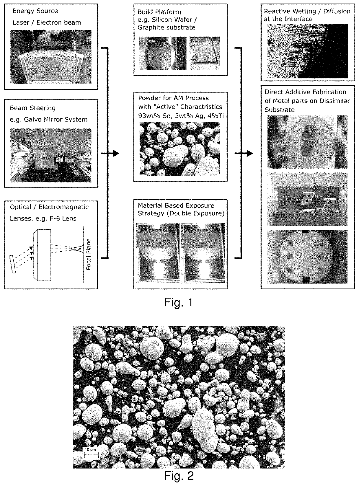
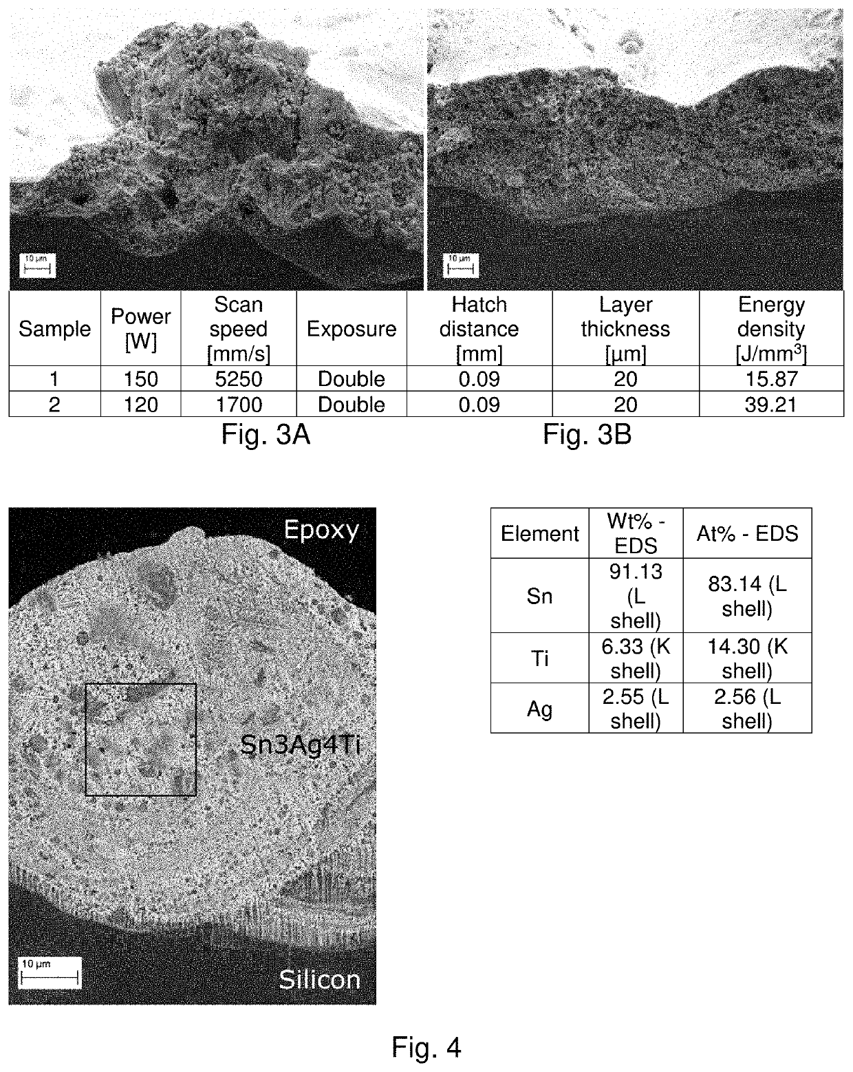
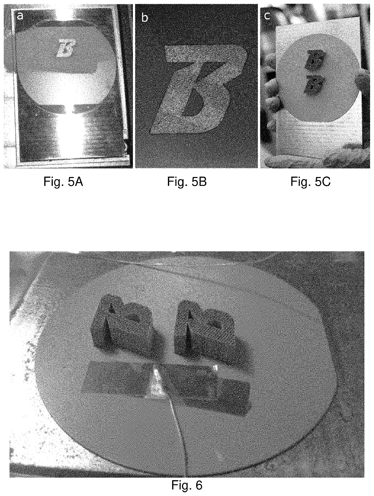
[0172]Metal powder may be deposited in fused layers a non-metal substrate by directed-energy powder fusion manufacturing. The energy source for this process can be from any focused energy sources, and popular sources include laser and electron beams. The powder can be deposited uniformly over an entire layer and then selectively melted, as is done in powder bed fusion processes, or it can be made with powder that is directly deposited onto the area of the part that is being exposed to the focused energy source, in the process typically referred to as directed energy deposition. The directed energy source may be steered or the sample stage may move the sample to selectively fuse powder where desired. This process is conducted in an inert environment, such as an Argon, N2, or vacuum environment to reduce oxidation risk.

[0173]A prototype of the technology employs a laser-powder bed fusion EOS M290 machine that possesses a 500 W peak 1064 nm Yb-fiber laser and high speed galvanometer mi...

example 2

[0234]The present technology provides an alternate technique for direct fabrication of heat transfer devices onto the chip by additive manufacturing, by building on recent hybrid bonding literature for interconnect manufacturing [98-101]. Previously lead solders, and more recently non-lead solders, have been used extensively in the electronic packaging industry to form interconnects, etc. However, reliability concerns are pushing the industry to move away from solders, towards a concept called hybrid bonding [94-97] which does not require solders. Hybrid bonding consists of multi-stage physical and chemical depositions onto a semiconductor device by employing photolithography-based techniques. This process produces a thin bonding layer via depositions that can then have features, like fins and microchannels, additively deposited via a powder-based laser melting process.

[0235]In this example, ˜50 nm of titanium is deposited onto the back of the semiconductor die by physical vapor dep...


PUM

PropertyMeasurementUnit
temperaturesaaaaaaaaaa

Abstract

A technique to additively print onto a dissimilar material, especially ceramics and glasses (e.g., semiconductors, graphite, diamond, other metals) is disclosed herein. The technique enables manufacture of heat removal devices and other deposited structures, especially on heat sensitive substrates. It also enables novel composites through additive manufacturing. The process enables rapid bonding, orders-of-magnitude faster than conventional techniques.

Description

CROSS REFERENCE TO RELATED APPLICATIONS[0001]The present application is a non-provisional of, and claims benefit or priority from each of U.S. Provisional Patent Application No. 62 / 806,901, filed Feb. 17, 2019, and U.S. Provisional Patent Application No. 62 / 717,444, filed Aug. 10, 2019, each of which is expressly incorporated herein by reference in its entirety.FIELD OF THE INVENTION[0002]The present invention relates to the field of additive manufacturing, and more particularly to additive manufacturing by controlled focused energy (e.g., laser or electron-beam) melting of particles, on a dissimilar substrate, specifically glasses and ceramics.BACKGROUND OF THE INVENTION[0003]Each reference cited herein is expressly incorporated by reference in its entirety, for all purposes.[0004]Additive manufacturing is well known. See the following U.S. patents and published patent applications: U.S. Pat. Nos. 10,000,023; 10,005,227; 10,005,228; 10,005,230; 10,005,237; 10,011,076; 10,011,089; 1...

Claims


Application Information

Patent Timeline
Patent Type & Authority Applications(United States)
IPC IPC(8): F28D15/00B32B15/01B32B7/12B33Y10/00B33Y80/00B33Y70/00F28F21/00F28F21/02F28F21/04F28F21/08
CPCB33Y80/00F28F21/04B33Y10/00F28F2210/00B32B15/01B23K26/342B33Y70/00F28F21/006F28F21/02F28F21/081B32B7/12F28D15/00B32B2457/00H01L21/4871H01L23/3736H01L23/3735F28D15/046F28F2255/18B22F2999/00B22F7/08B22F10/28B22F10/36B33Y70/10H01L21/283H01L23/367
Inventor SCHIFFRES, SCOTT N.AZIZI, ARAD
Owner THE RES FOUND OF STATE UNIV OF NEW YORK
Why Eureka
Try Eureka