
Omnidirectional polarization independent all-dielectric light trapping scheme

a technology of all-dielectric light and trapping scheme, applied in the field of photovoltaic cells, can solve the problems of increasing surface recombination, affecting the efficiency of solar cells, and not being able to achieve manipulation, so as to reduce recombination and refractory losses, improve the efficiencies and lifespan of flexible solar cells

Pending Publication Date: 2020-05-07
UNIV OF CENT FLORIDA RES FOUND INC
View PDF1 Cites 2 Cited by
  • Summary
  • Abstract
  • Description
  • Claims
  • Application Information

AI Technical Summary

Benefits of technology

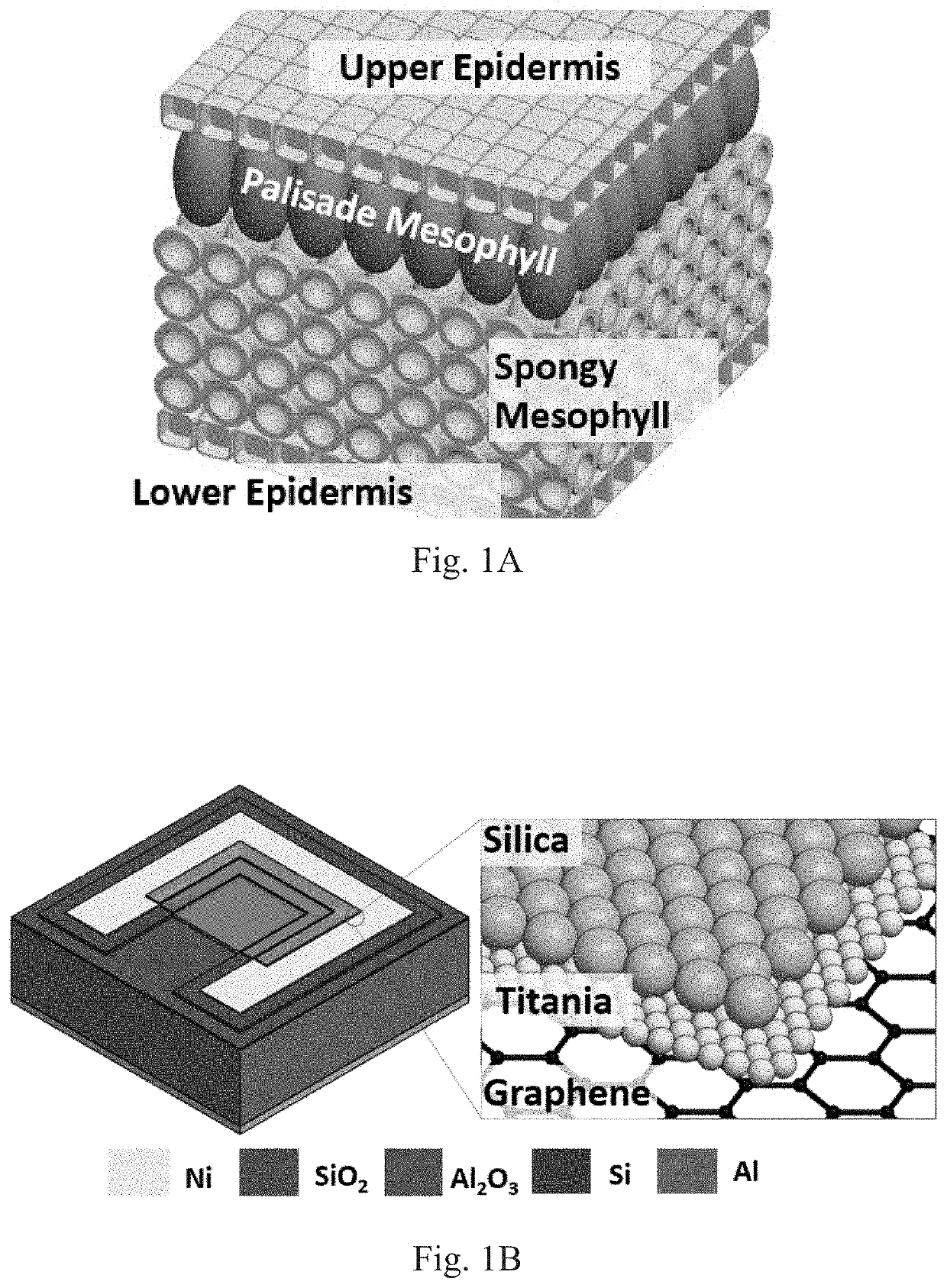
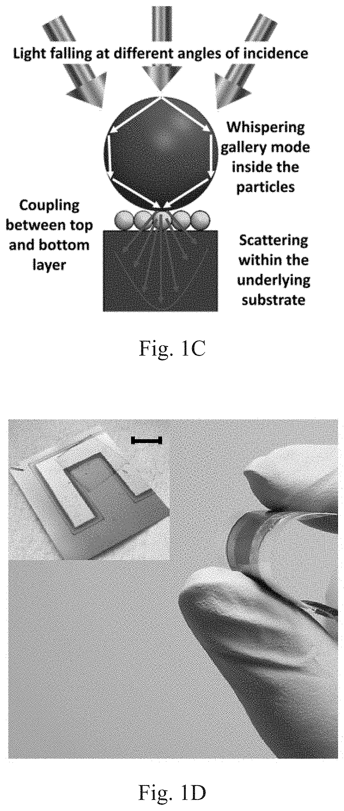
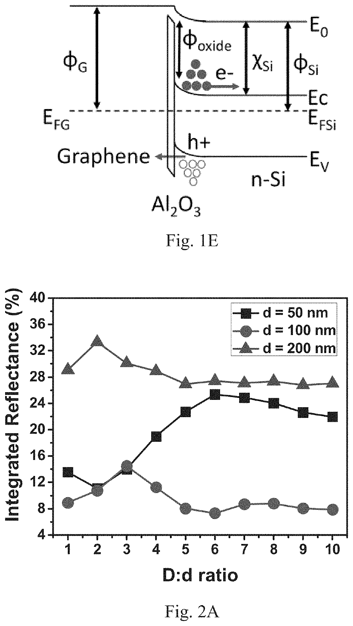
This patent describes a way to improve the efficiency and lifespan of flexible solar cells by using a special design that redirects light and reduces refractory loss. The design includes a layer made of nanoparticles with different optical properties. The first layer is made of silica nanospheres and the second layer is made of titania nanospheres. The difference in height between the layers creates a cavity where light can be trapped and redirected with reduced loss. Overall, this design helps increase the amount of sunlight that can be captured and converted into electricity by the solar cell.

Problems solved by technology

For an ultrathin silicon substrate, manipulation of the incoming light, such as collimation, scattering, focusing, and funneling, is needed, which can lead to significant absorption enhancement in the active layer; however, the light manipulation may not take place due to the antireflective coating.
However, structuring the active silicon substrate to enhance light trapping maximizes the surface area of the solar cell, leading to an increase in surface recombination, which is detrimental to the solar cell efficiency.
As such, while such engineered structures increase the optical response of the solar cell, the surface degradation of the cell is such that the optical gains do not translate effectively into electrical gains for the cell.
These deformations modify the electronic and optical properties of the graphene film, and cause discontinuities in the Gr / Si heterojunction.
When graphene is transferred onto a silicon substrate bearing ordered pyramidal pillars, microwrinkles with a height of several micrometers are formed, [32], which reduces solar cell performance.
Thirdly, metallic nanostructures at the back side of the surface aids in propagating light in the plane of the semiconductor, increasing the light's probability for getting absorbed in the active solar absorber.
While all three configurations enable unrivalled light absorption enhancement in the solar absorber, a significant part of this energy is always dissipated due to the ohmic loss, leading to joule heating in metal entities.
Therefore, plasmonic losses present a major hurdle in utilizing the energy effectively, necessitating the development of highly efficient solar cells.
However, WGM resonators used for solar cell applications must have a sufficiently low quality factor (Q), low frequency selectivity, and strong in-coupling.
Furthermore, where a definition or use of a term in a reference, which is incorporated by reference herein, is inconsistent or contrary to the definition of that term provided herein, the definition of that term provided herein applies and the definition of that term in the reference does not apply.

Method used


Image

  • Omnidirectional polarization independent all-dielectric light trapping scheme
  • Omnidirectional polarization independent all-dielectric light trapping scheme
  • Omnidirectional polarization independent all-dielectric light trapping scheme

Examples


Embodiment Construction

[0065]In the following detailed description of the preferred embodiments, reference is made to the accompanying drawings, which form a part thereof, and within which are shown by way of illustration specific embodiments by which the invention may be practiced. It is to be understood that other embodiments may be utilized and structural changes may be made without departing from the scope of the invention.

[0066]As used in this specification and the appended claims, the singular forms “a,”“an,” and “the” include plural referents unless the content clearly dictates otherwise. As used in this specification and the appended claims, the term “or” is generally employed in its sense including “and / or” unless the context clearly dictates otherwise.

[0067]The present invention includes a leaf inspired biomimetic light trapping scheme for ultrathin flexible solar cells, such as graphene silicon (Gr / Si) Schottky junction solar cell. The light trapping scheme is all-dielectric lossless hierarchic...


PUM

PropertyMeasurementUnit
heightaaaaaaaaaa
thickaaaaaaaaaa
angleaaaaaaaaaa

Abstract

A leaf inspired biomimetic light trapping scheme for ultrathin flexible graphene silicon Schottky junction solar cell. An all-dielectric approach comprising of lossless silica and titania nanoparticles is used for mimicking the two essential light trapping mechanisms of a leaf: (1) focusing and waveguiding and (2) scattering. The light trapping scheme uses two optically tuned layers and does not require any nano-structuring of the active silicon substrate, thereby ensuring that the optical gain is not offset due to recombination losses.

Description

CROSS-REFERENCE TO RELATED APPLICATIONS[0001]This nonprovisional application is a continuation of and claims priority to provisional application No. 62 / 756,669, entitled “Omnidirectional polarization independent all-dielectric light trapping scheme,” filed Nov. 7, 2018, by the same inventors, the entirety of which is incorporated herein by reference.BACKGROUND OF THE INVENTION1. Field of the Invention[0002]This invention relates, generally, to photovoltaic cells. More specifically, it relates to a light trapping scheme for photovoltaic / solar cells.2. Brief Description of the Prior Art[0003]With the need for emerging photovoltaic cells to be fabricated on bendable supports and capable of high-speed, roll-to-roll processing, silicon (Si)—the most widely used material in solar cells—is gradually evolving towards a flexible future based on monocrystalline substrates. [1-3]. Flexible monocrystalline silicon photovoltaics will need a paradigm shift in terms of wafer manufacturing, sawing ...

Claims


Application Information

Patent Timeline
Patent Type & Authority Applications(United States)
IPC IPC(8): H01L51/44H01L31/108H01L31/20C01B33/12G02B5/30H01L31/0216
CPCC01P2004/64H01L31/108C01B33/12H01L31/204H01L31/02167G02B5/3008H01L51/447H01L31/047H01L31/02168H01L31/028Y02E10/547Y02E10/549Y02E10/52H10K30/87
Inventor ROY, TANIADAS, SONALI
Owner UNIV OF CENT FLORIDA RES FOUND INC
Learn More