Top-Gate Self-Aligned Indium -Zinc Oxide Thin-Film Transistor and Manufacturing Method Therefore

a technology of indium-zinc oxide and self-alignment, which is applied in the field of semiconductors, can solve the problems of poor thermal stability of the treated source and drain region, unfriendly to high-resolution displays and system-on-panel (sop) technology, and weak device scalability, so as to reduce production costs, small parasitic capacitance, and strong device scalability

Active Publication Date: 2020-08-13
SOUTH CHINA UNIV OF TECH
View PDF0 Cites 0 Cited by
  • Summary
  • Abstract
  • Description
  • Claims
  • Application Information

AI Technical Summary

Benefits of technology

[0029]The transistor of the present disclosure has the beneficial effects that: the transistor comprises the substrate, the buffer layer, the ITZO thin film, the gate dielectric layer, the conductive thin film, the passivation layer, the gate, source and drain contact electrodes; and the transistor has a TG-SA structure, which can overcome the problems of large parasitic capacitance and weak device scalability in a traditional bottom-gate ITZO TFT. Moreover, the transistor of the present disclosure has the advantages of small parasitic capacitance and strong device scalability.
[0030]The method of the present disclosure has the beneficial effects that: the method comprises the following step: depositing the gate dielectric layer on the patterned ITZO thin film by using the first chemical vapor deposition method; etching the gate dielectric layer by using the patterned conductive thin film as the mask, and performing the first annealing; depositing the passivation layer on the conductive thin film and the ITZO thin film by using the second chemical vapor deposition method; and performing the second annealing. The precursor used in the first chemical vapor deposition method comprises the alkoxysilane or the mixed gas source of alkoxysilane and in...

Problems solved by technology

However, the bottom-gate devices suffer from large parasitic capacitance and weak device scalability, thus being unfriendly to high-resolution displays and system-on-panel (SOP) technology.
Therefore, these TFTs with the p...

Method used


Image

  • Top-Gate Self-Aligned Indium -Zinc Oxide Thin-Film Transistor and Manufacturing Method Therefore
  • Top-Gate Self-Aligned Indium -Zinc Oxide Thin-Film Transistor and Manufacturing Method Therefore
  • Top-Gate Self-Aligned Indium -Zinc Oxide Thin-Film Transistor and Manufacturing Method Therefore

Examples


embodiment 1

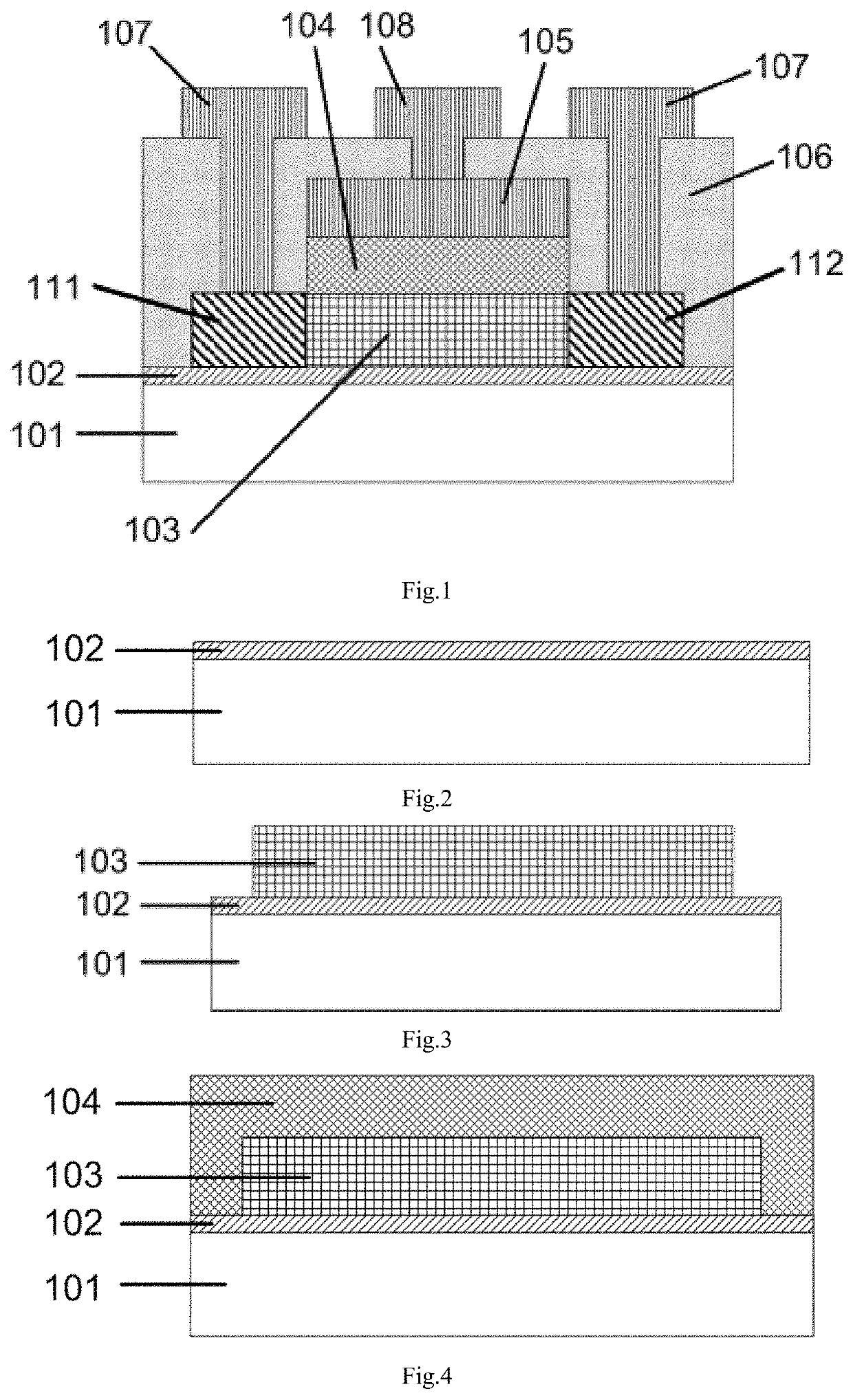
[0059]With reference to FIG. 1, a TG-SA ITZO TFT comprises a substrate 101; a buffer layer 102 provided on the substrate 101, wherein the buffer layer 102 is composed of silicon dioxide; an ITZO thin film 103 provided on the buffer layer 102, wherein the ITZO thin film 103 comprises two low-resistivity source and drain regions (a first low-resistivity source and drain region 111, and a second low-resistivity source and drain region 112) and one high-resistivity channel region; a gate dielectric layer 104 provided on the ITZO thin film 103, wherein the gate dielectric layer 104 is composed of silicon dioxide; a conductive thin film 105 provided on the gate dielectric layer 104, wherein the conductive thin film 105 is composed of metallic aluminum; a passivation layer 106 provided on the conductive thin film 105, wherein the passivation layer 106 is composed of silicon dioxide and comprises two contact holes of a source and a drain and one contact hole of a gate, the conductive thin f...

embodiment 2

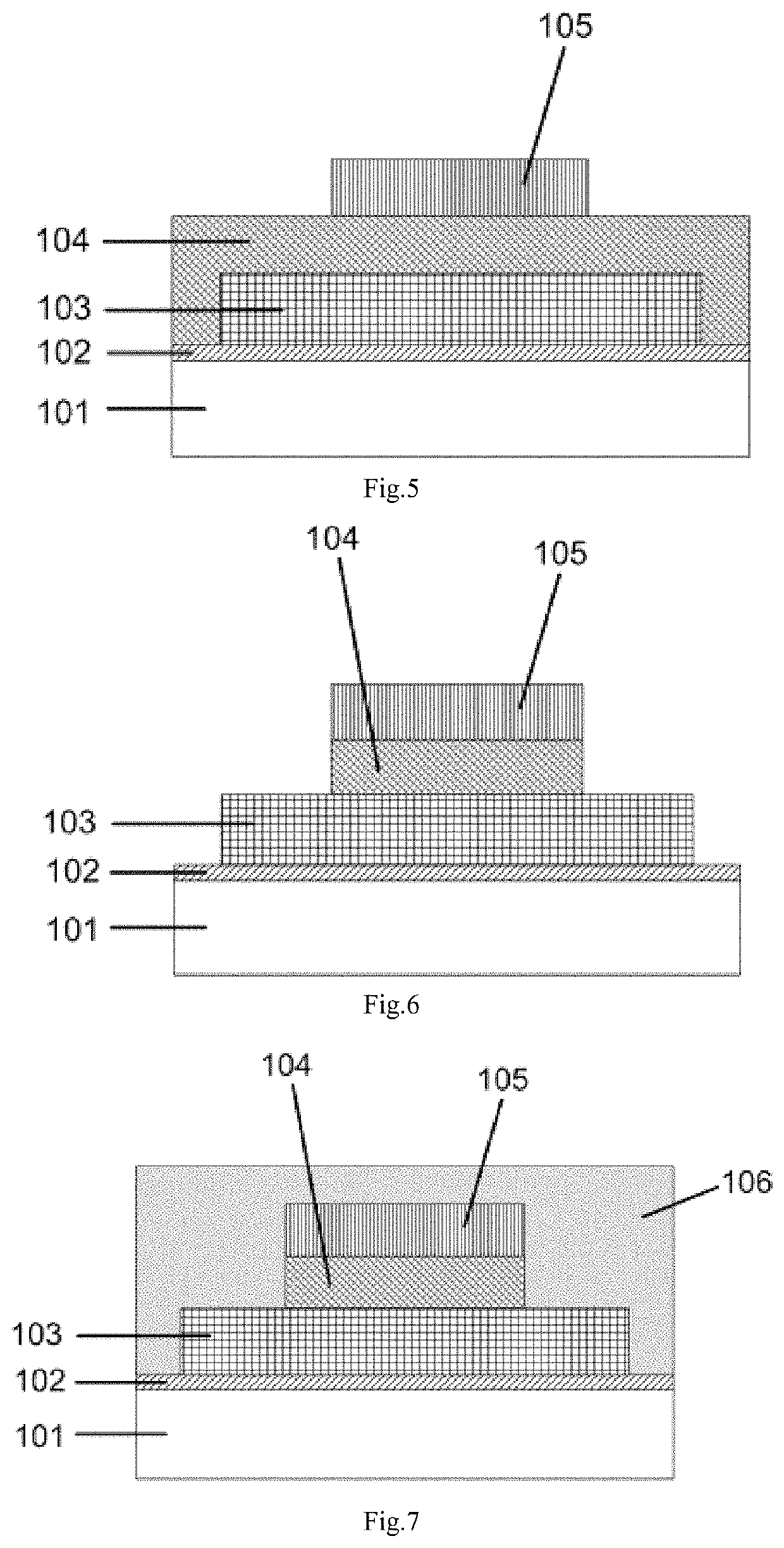
[0061]With reference to FIG. 1 to FIG. 7, a method for manufacturing a TG-SA ITZO TFT comprises the following steps:

[0062]S1, depositing a buffer layer 102 on a substrate 101 by using a thermal oxidation method, as shown in FIG. 2;

[0063]S2, depositing an ITZO thin film 103 on the buffer layer 102 by using a magnetron sputtering method, as shown in FIG. 3; wherein the magnetron sputtering method is a DC magnetron sputtering method and a RF magnetron sputtering method, and an ITO target material and a ZnO target material are used as target materials in the magnetron sputtering method; a DC power supply is used when the ITO target material is sputtered, and an input power of the DC power supply is 120 W; a RF power supply is used when the ZnO target material is sputtered, and an input power of the RF power supply is 150 W; a reaction atmosphere is oxygen and argon, and a working pressure is 3 mTorr;

[0064]S3, performing photolithography and wet etch on the ITZO thin film 103 to pattern ...


PUM


Abstract

The TG-SA ITZO TFT comprises a substrate, a buffer layer, an ITZO thin film, a gate dielectric layer, a conductive thin film, a passivation layer, gate, source and drain contact electrodes. The transistor has a TG-SA structure, which can address the issues of larger parasitic capacitance and weaker device scalability in a traditional bottom-gate counterpart. When depositing the gate dielectric layer and the passivation layer, different gas sources and annealing conditions are used, such that the ITZO thin film region contacted with and covered by the gate dielectric layer shows a high-resistivity state, the ITZO thin film region contacted with and covered by the passivation layer shows a low-resistivity state, thereby forming a high-resistivity channel region and low-resistivity conductive source and drain regions, and addressing the thermal instability issue.

Description

FIELD OF THE INVENTION[0001]The present disclosure relates to the technical field of semiconductors, and more particularly, to a top-gate self-aligned (TGSA) indium-tin-zinc oxide (ITZO) thin-film transistor (TFT) and manufacturing method thereof.BACKGROUND OF THE INVENTION[0002]Explanation of terms[0003]Precursor: refers to a precursor or a raw material for synthesizing some substance.[0004]With the development of next-generation active-matrix organic-light-emitting-diode (AMOLED) display technology, metal oxide thin-film transistor (TFTs) have attracted great attention and been intensively studied, wherein bottom-gate ITZOTFTs are one of the most representative example. However, the bottom-gate devices suffer from large parasitic capacitance and weak device scalability, thus being unfriendly to high-resolution displays and system-on-panel (SOP) technology. So far, some of research groups have developed a type of top-gate self-aligned (TG-SA) TFTs with smaller parasitic capacitance...

Claims


Application Information

Patent Timeline
IPC IPC(8): H01L27/12
CPCH01L27/1251H01L27/1225H01L27/127H01L27/1248H01L29/66969H01L29/7869H01L21/02554
Inventor CHEN, RONGSHENGDENG, SUNBINKWOK, HOISING
Owner SOUTH CHINA UNIV OF TECH
Why Eureka
Try Eureka