Adjustable hyperspectral detection chip enhanced by multi-resonance plasmonic mechanism

Active Publication Date: 2021-02-04
SOUTHEAST UNIV
View PDF0 Cites 3 Cited by
  • Summary
  • Abstract
  • Description
  • Claims
  • Application Information

AI Technical Summary

Benefits of technology

[0018]2. An adjustable hyperspectral detection chip enhanced by a multi-resonance plasmonic mechanism is provided. By utilizing strong ultra-narrow band absorption of a plasmonic nanonail structure with a multi-resonance enhancement effect and strong sensitivity of a resonance peak thereof to a short-range dielectric environment, hyperspectral detection of an infrared band photo-induced hot carrier mechanism is implemented, so that a problem that spectral resolution of an existing infrared optoelectronic detection chip is low can be overcome, and spectral resolution is better than 1 nanometer.
[00

Problems solved by technology

However, detection wavelengths of the existing conventional infrared photodetectors are limited by a band gap of a semiconductor material and a longer band cannot be detected.
In addition, a photodetector usually performs lig

Method used


Image

  • Adjustable hyperspectral detection chip enhanced by multi-resonance plasmonic mechanism
  • Adjustable hyperspectral detection chip enhanced by multi-resonance plasmonic mechanism
  • Adjustable hyperspectral detection chip enhanced by multi-resonance plasmonic mechanism

Examples


embodiment

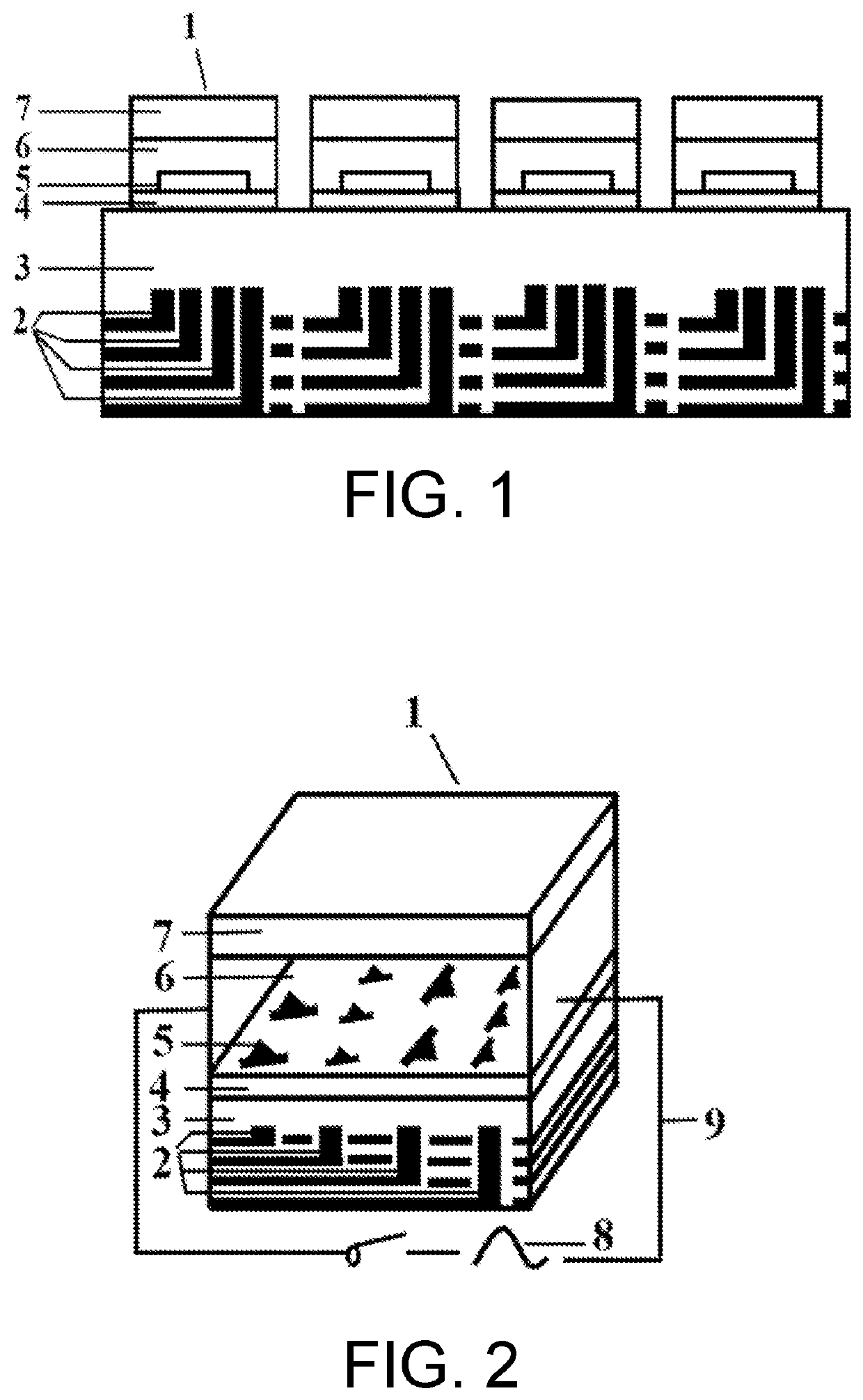
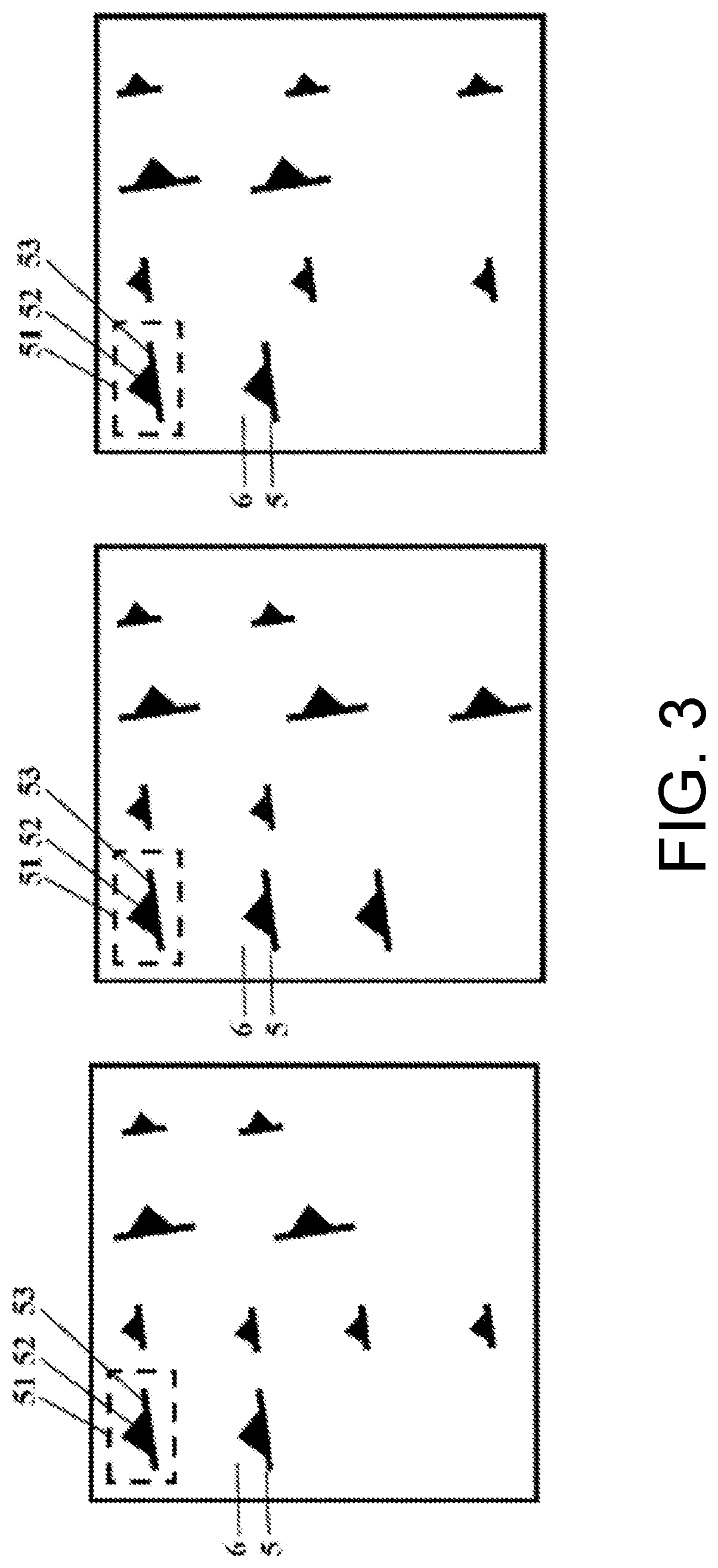
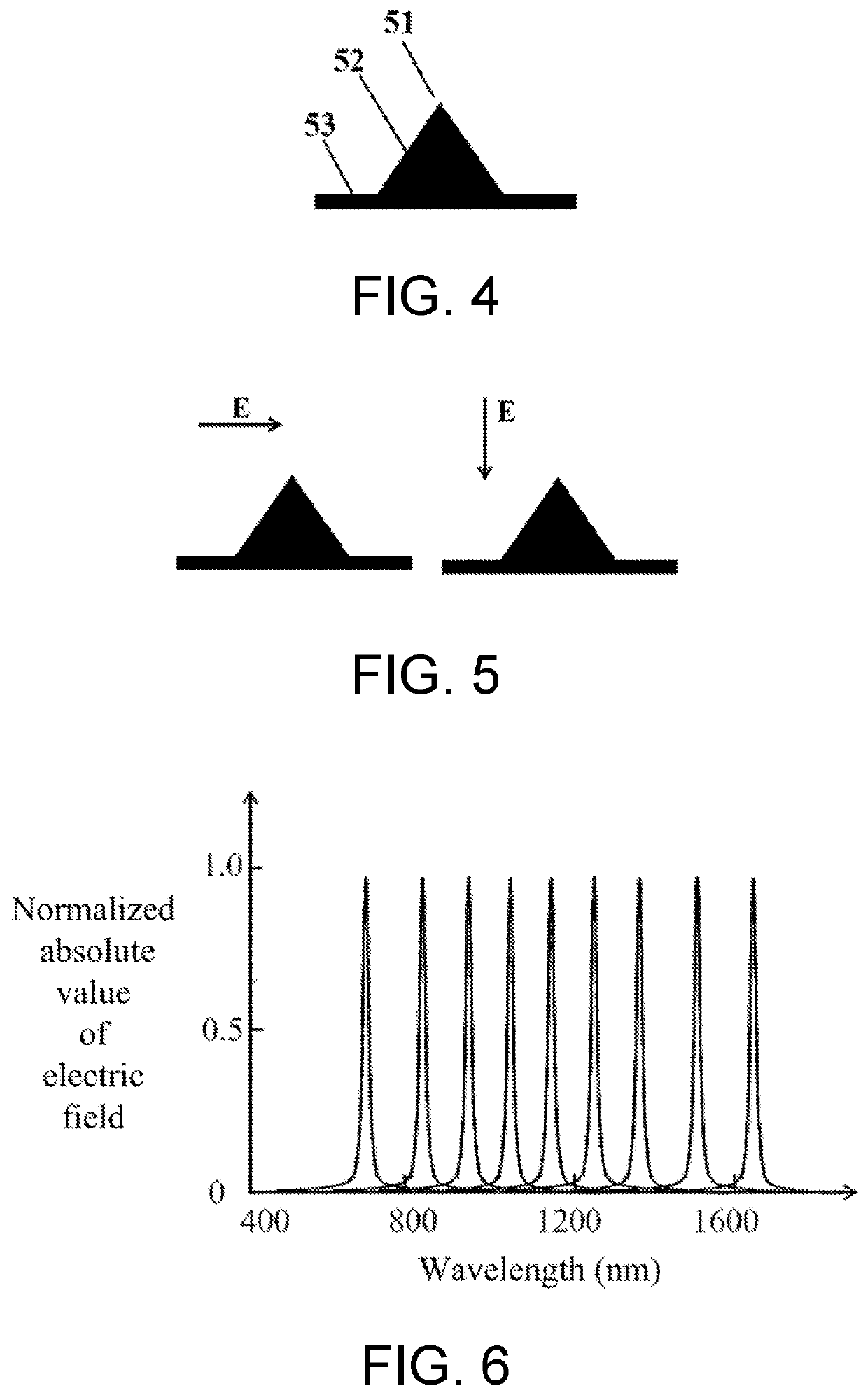
[0035]A detection unit structure of an adjustable hyperspectral detection chip enhanced by a multi-resonance plasmonic mechanism is shown in FIG. 1, including an aluminum electrode 2, an n-type silicon 3, a silicon-dioxide layer 4, a silver nanonail array 5, an electro-optical control material layer 6, an indium tin oxide electrode 7, a periodical voltage control signal 8, and a driving circuit 9. The silver nanonail array 5 is loaded inside the electro-optical control material layer 6. The silver nanonail array 5 is formed by silver nanonails 51 arranged periodically, and the silver nanonail 51 includes two parts: a silver triangular nanoplate 52 and a silver nanorod 53, and the driving circuit 9 is connected to both sides of the control material layer 6.

[0036]When light is irradiated on the detection unit, carriers cross the Schottky barrier to form a photocurrent by using a heterojunction between the n-type silicon 3 and the silver nanonail array 5 based on a plasmon-induced hot ...


PUM


Abstract

An adjustable hyperspectral detection chip enhanced by a multi-resonance plasmonic mechanism. The detection chip consists of an array of metal nanonail resonator detection units. Each detection unit (1) comprises: a bottom electrode (2), a semiconductor material layer (3), a spacer layer (4), a nanonail array (5), a control material layer (6), a top electrode (7), a peripheral control signal (8), and a driving circuit (9). The positional relationship from top to bottom is the top electrode (7), the control material layer (6), the nanonail array (5), the spacer layer (4), the semiconductor material layer (3), and the bottom electrode (2). The nanonail array (5) is loaded inside the control material layer (6), and the peripheral control signal (8) and the driving circuit (9) are connected to both sides of the control material layer (6).

Description

BACKGROUNDTechnical Field[0001]The present invention belongs to the fields such as the field of infrared detectors and the field of metal nanomaterials, and specifically, to an adjustable hyperspectral detection chip enhanced by a multi-resonance plasmonic mechanism.Description of Related Art[0002]In the hyperspectral imaging detection technology, a hyperspectral image with specific spectral resolution is used for target detection. Compared with the conventional single-wide band optoelectronic detection technology, the hyperspectral imaging detection technology requires a combination of the imaging technology and spectral measurement technology to obtain two-dimensional spatial information and spectral radiation information with distribution of wavelengths. Only by implementing high-precision resolution of target spectral information and a target space image, can accuracy of target detection be improved, functions of conventional detection technologies be expanded, and application r...

Claims


Application Information

Patent Timeline
IPC IPC(8): G01J3/447G01J3/28H01L31/0352H01L31/0232H01L31/101H01L27/146
CPCG01J3/447G01J3/2823H01L31/0352G01J2003/2826H01L31/1013H01L27/14625H01L31/02327H01L27/14601H01L27/14649H01L31/108
Inventor ZHANG, TONGSU, DANXIONG, MENGSHAN, FENGZHANG, XIAOYANG
Owner SOUTHEAST UNIV
Why Eureka
Try Eureka