Methods And Systems For Semiconductor Metrology Based On Wavelength Resolved Soft X-Ray Reflectometry

a technology of soft x-ray reflectometry and wavelength resolution, applied in the direction of material analysis using radiation diffraction, semiconductor/solid-state device testing/measurement, instruments, etc., can solve the problems of limited information concerning the composition and shape of nanostructure materials, difficult characterization, and limited information, so as to improve measurement accuracy and throughput , the effect of wide rang

Active Publication Date: 2021-03-04
KLA TENCOR TECH CORP
View PDF0 Cites 7 Cited by
  • Summary
  • Abstract
  • Description
  • Claims
  • Application Information

AI Technical Summary

Benefits of technology

[0018]Methods and systems for measuring structural and material characteristics of semiconductor structures based on wavelength resolved, soft x-ray reflectometry (WR-SXR) at multiple diffraction orders are presented herein. The methods and systems described her

Problems solved by technology

As devices (e.g., logic and memory devices) move toward smaller nanometer-scale dimensions, characterization becomes more difficult.
Devices incorporating complex three-dimensional geometry and materials with diverse physical properties contribute to characterization difficulty.
Accurate information concerning the material composition and shape of nanostructures is limited in the process development environment of a leading-edge front-end semiconductor fabrication facility.
With limited knowledge of material composition and shape of nanostructures available apriori, measurement recipe development and validation is a slow and tedious process.
For example, cross-sectional transmission electron microscopy (TEM) images are used to guide optical scatterometry model development, but TEM imaging is slow and destructive.
Furthermore, when absorbing materials are present in the structure under measurement, penetration and scattering of illumination light in the optical region (e.g., 0.5 - 10ev) limits the utility of conventional optical metrology systems.
Similarly, electron beam based metrology systems struggle to penetrate semiconductor structures due to absorption and scattering of the illuminating, backscattered, and secondary emission electrons.
Atomic force microscopes (AFM) and scanning-tunneling microscopes (STM) are able to a

Method used


Image

  • Methods And Systems For Semiconductor Metrology Based On Wavelength Resolved Soft X-Ray Reflectometry
  • Methods And Systems For Semiconductor Metrology Based On Wavelength Resolved Soft X-Ray Reflectometry
  • Methods And Systems For Semiconductor Metrology Based On Wavelength Resolved Soft X-Ray Reflectometry

Examples


Embodiment Construction

[0050]Reference will now be made in detail to background examples and some embodiments of the invention, examples of which are illustrated in the accompanying drawings.

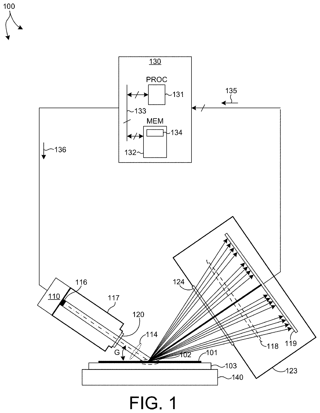
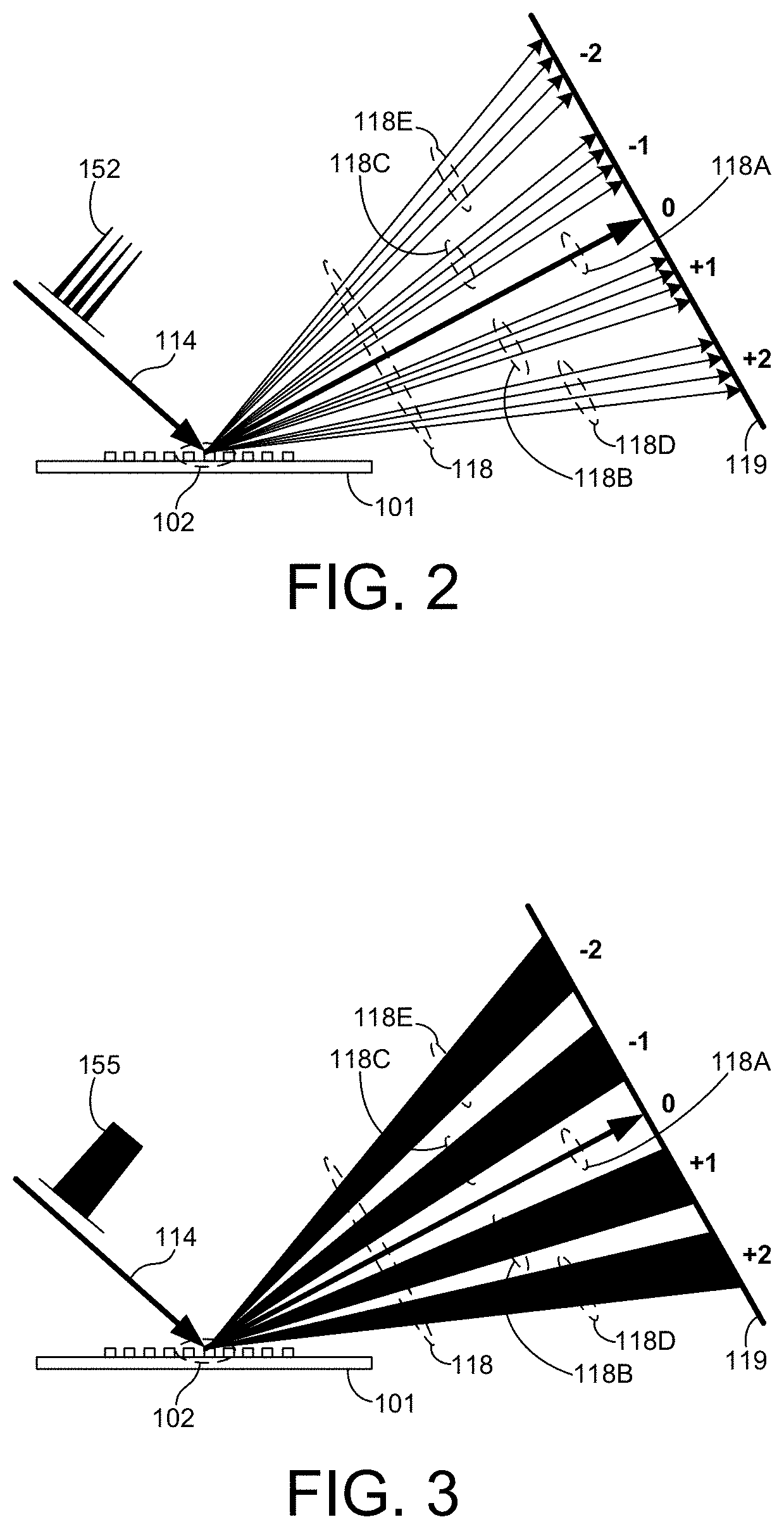
[0051]Methods and systems for measuring structural and material characteristics (e.g., material composition, dimensional characteristics of structures and films, etc.) of semiconductor structures associated with different semiconductor fabrication processes based on x-ray illumination are presented. More specifically, methods and systems for performing measurements of semiconductor structures based on wavelength resolved, soft x-ray reflectometry (WR-SXR) at multiple diffraction orders are presented herein. The methods and systems described herein provide simultaneous, high throughput measurements over multiple diffraction orders with broad spectral width. The availability of wavelength resolved signal information at each of the multiple diffraction orders improves measurement accuracy and throughput.

[0052]In general,...


PUM


Abstract

Methods and systems for measuring structural and material characteristics of semiconductor structures based on wavelength resolved, soft x-ray reflectometry (WR-SXR) at multiple diffraction orders are presented. WR-SXR measurements are simultaneous, high throughput measurements over multiple diffraction orders with broad spectral width. The availability of wavelength resolved signal information at each of the multiple diffraction orders improves measurement accuracy and throughput. Each non-zero diffraction order includes multiple measurement points, each different measurement point associated with a different wavelength. In some embodiments, WR-SXR measurements are performed with x-ray radiation energy in a range of 10-5,000 electron volts at grazing angles of incidence in a range of 1-45 degrees. In some embodiments, the illumination beam is controlled to have relatively high divergence in one direction and relatively low divergence in a second direction, orthogonal to the first direction. In some embodiments, multiple detectors are employed, each detecting different diffraction orders.

Description

TECHNICAL FIELD[0001]The described embodiments relate to x-ray metrology systems and methods, and more particularly to methods and systems for improved measurement accuracy.BACKGROUND INFORMATION[0002]Semiconductor devices such as logic and memory devices are typically fabricated by a sequence of processing steps applied to a specimen. The various features and multiple structural levels of the semiconductor devices are formed by these processing steps. For example, lithography among others is one semiconductor fabrication process that involves generating a pattern on a semiconductor wafer. Additional examples of semiconductor fabrication processes include, but are not limited to, chemical-mechanical polishing, etch, deposition, and ion implantation. Multiple semiconductor devices may be fabricated on a single semiconductor wafer and then separated into individual semiconductor devices.[0003]Metrology processes are used at various steps during a semiconductor manufacturing process to...

Claims


Application Information

Patent Timeline
IPC IPC(8): G01N23/2206G01N23/2204G01N23/207H01L21/66
CPCG01N23/2206G01N23/2204G01N23/083H01L22/12G01N2223/6116G01N23/2076G01N23/20008G01N23/205G01N2223/0561G01N2223/1016G01N2223/645G01N2223/052G01N2223/206G01N23/20
Inventor KUZNETSOV, ALEXANDERCHANG, CHAO
Owner KLA TENCOR TECH CORP
Why Eureka
Try Eureka