In this context, prior art methods of doping have strong limitations, because they do not allow the doping of
silicon to be carried out in such a way that it follows the 3D nanostructured surfaces, i.e. they do not allow to make ‘conformal’ doping.
In addition, prior art methods need to use expensive equipment and materials in order to avoid the formation of structural defects within the
silicon, typically only partially solved by subsequent heating, the uncontrolled formation of precipitates and poor manageability in the realization of specific applications such as ultra-thin junctions (under 10 nm).
However, a determining aspect that has prevented a wide and extensive development of the methodologies described in the document by Ho at al. and in the
patent application US2012 / 0003826A1 in the industrial field is linked to the problem that the atoms constituting the molecule can diffuse together with the dopant atoms in the first sample
layers.
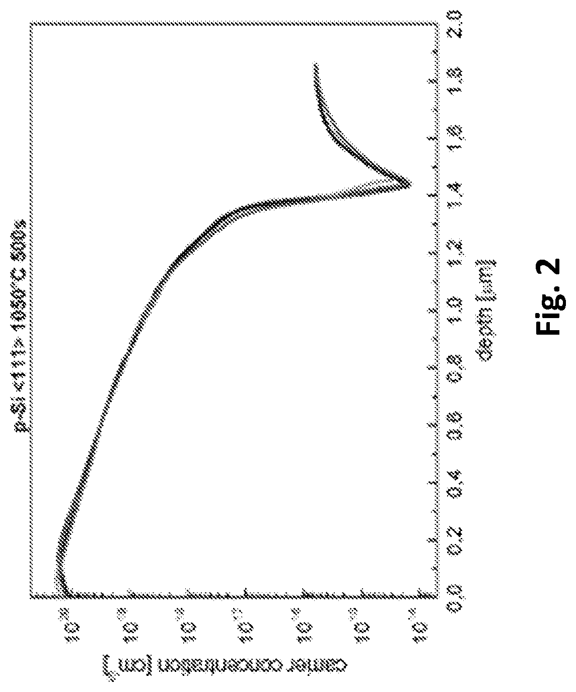
It is known indeed that carbon is identified as a benign contaminant for some devices, such as MOS and bipolar devices, but in others, such as
high voltage diodes and transistors, at concentrations higher than 5×1016 cm−3, it forms structural defects and electronic deep traps in the Si bandgap and consequently it deteriorates the device electrical properties.
Although this layer is confined to the surface, this has been identified as one of the limits of the technique.
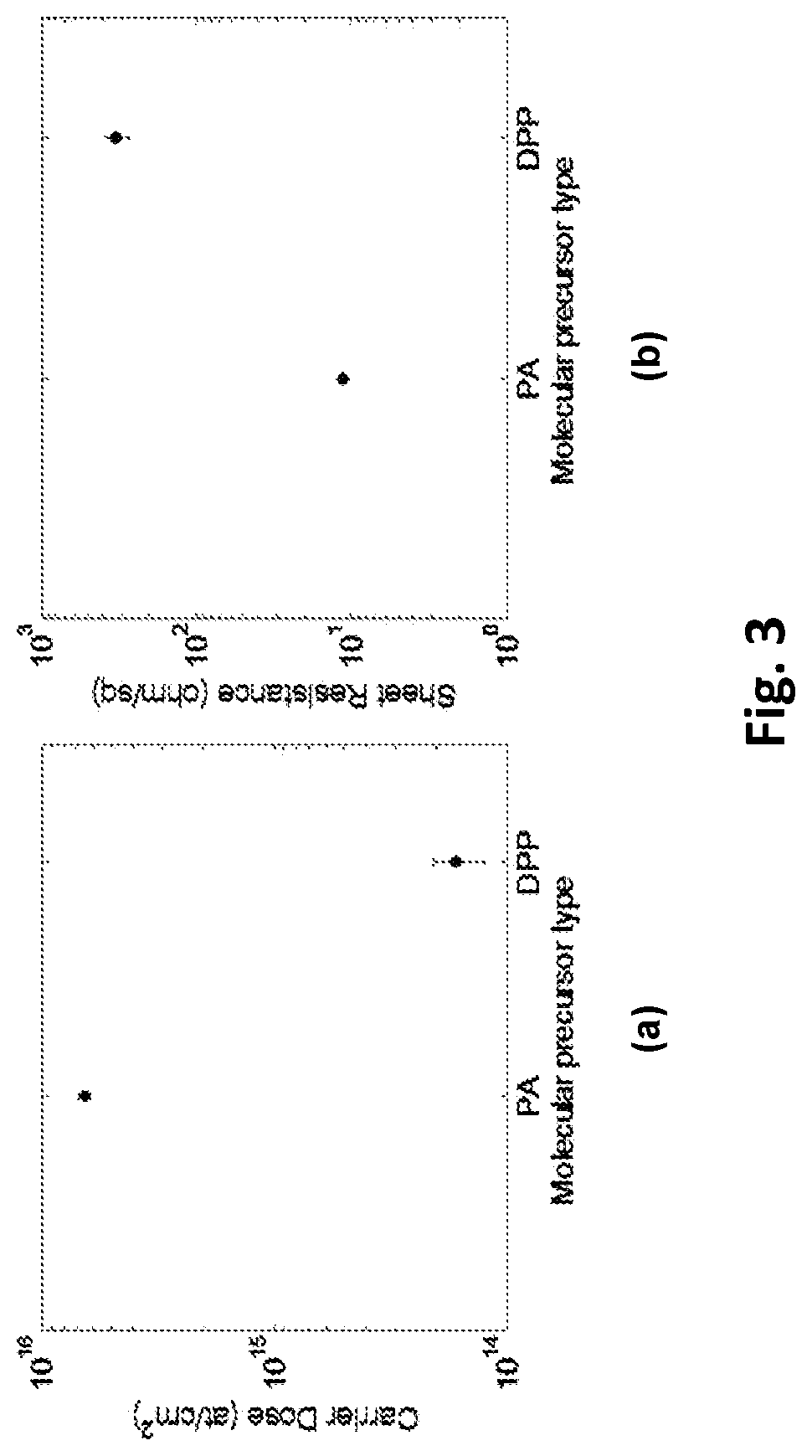
Some works in the literature have proposed the use of alternative precursors to the DPP to reduce the carbon
impact, but always without eliminating it, e.g. as disclosed in “Behavior of phosphorous and contaminants from molecular doping combined with a conventional spike annealing method” by Yasuo Shimizu et al., published on 27 Nov. 2013, Nanoscale, 2014, 6, 706, and in document US 2005 / 181566 A1, providing further inconveniences which made the technological process less attractive.
However, this approach lacks uniformity in terms of dopants distribution, cost-efficiency due to a
laser source necessity and it is also time-consuming due to the iterative and selective utilization of the
laser beam.
Due to the limited dimension of the
laser focal spot, non-uniform changes in the physical and chemical properties of the implanted substrates are generated.
Moreover, laser activation needs dedicated facilities in terms of light sources and special controls which are more expensive and more complicated than other standard thermal annealing.
Furthermore, this kind of
beam energy annealing is not effective to achieve a conformal doping on hidden surfaces of complex tri-dimensional structures, such as nanostructured, porous or hollow ones, which would not be achieved by a laser beam activation.
The step of dipping the semiconductor in an aqueous ambient temperature solution does not ensure any fine
controllability of the dopant
coating achieved in the doping process.
Furthermore,
butanol, as well as
ethanol and
methanol, has several C—H bonds in a single molecule thus the doped sample obtained is a carbon contaminated sample, moreover a
phosphorus silicate glass (PSG) layer is formed on the sample surface which needs to be removed by a further expensive process.

