

Light absorption layer and manufacturing method therefor, photoelectric conversion element, and intermediate-band solar cell
a technology of light absorption layer and manufacturing method, which is applied in the direction of luminescent compositions, chemistry apparatus and processes, and titanium compounds, etc., can solve the problems of inability to improve the inhibit the growth of bulk semiconductor crystals, and many voids in the produced light absorption layer, etc., to achieve excellent quantum efficiency of two-step light absorption
- Summary
- Abstract
- Description
- Claims
- Application Information
AI Technical Summary
Benefits of technology
Problems solved by technology
Method used
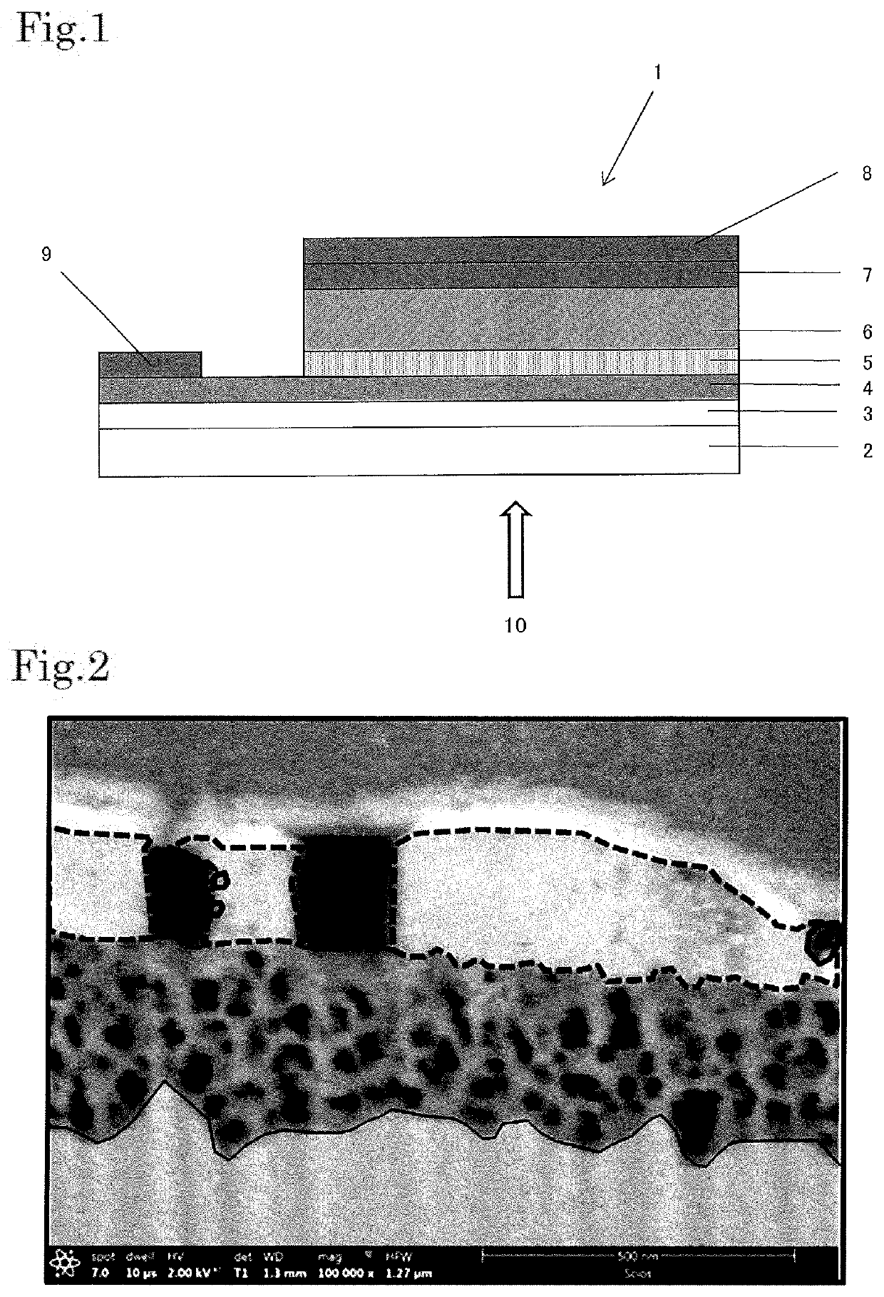
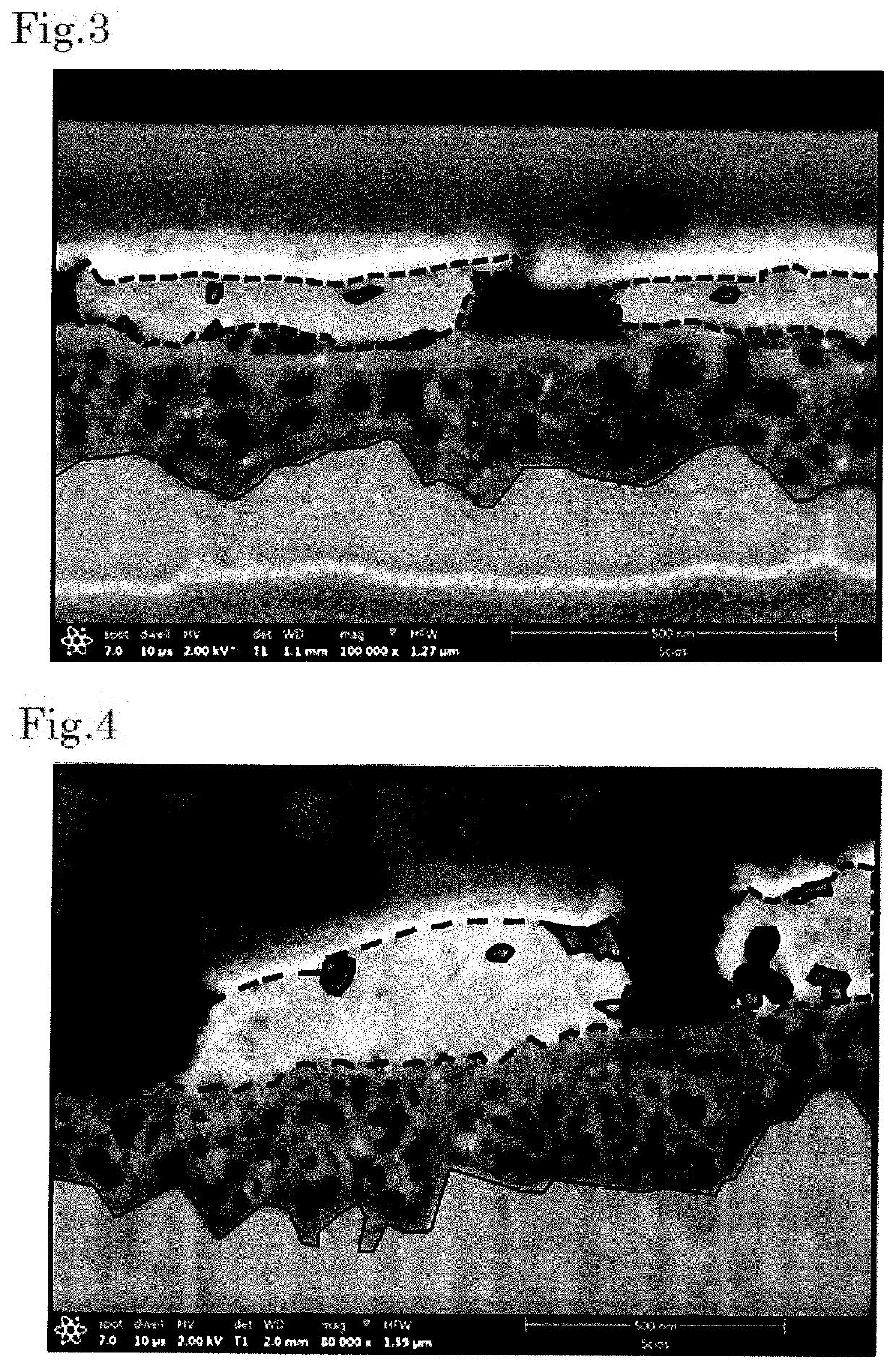
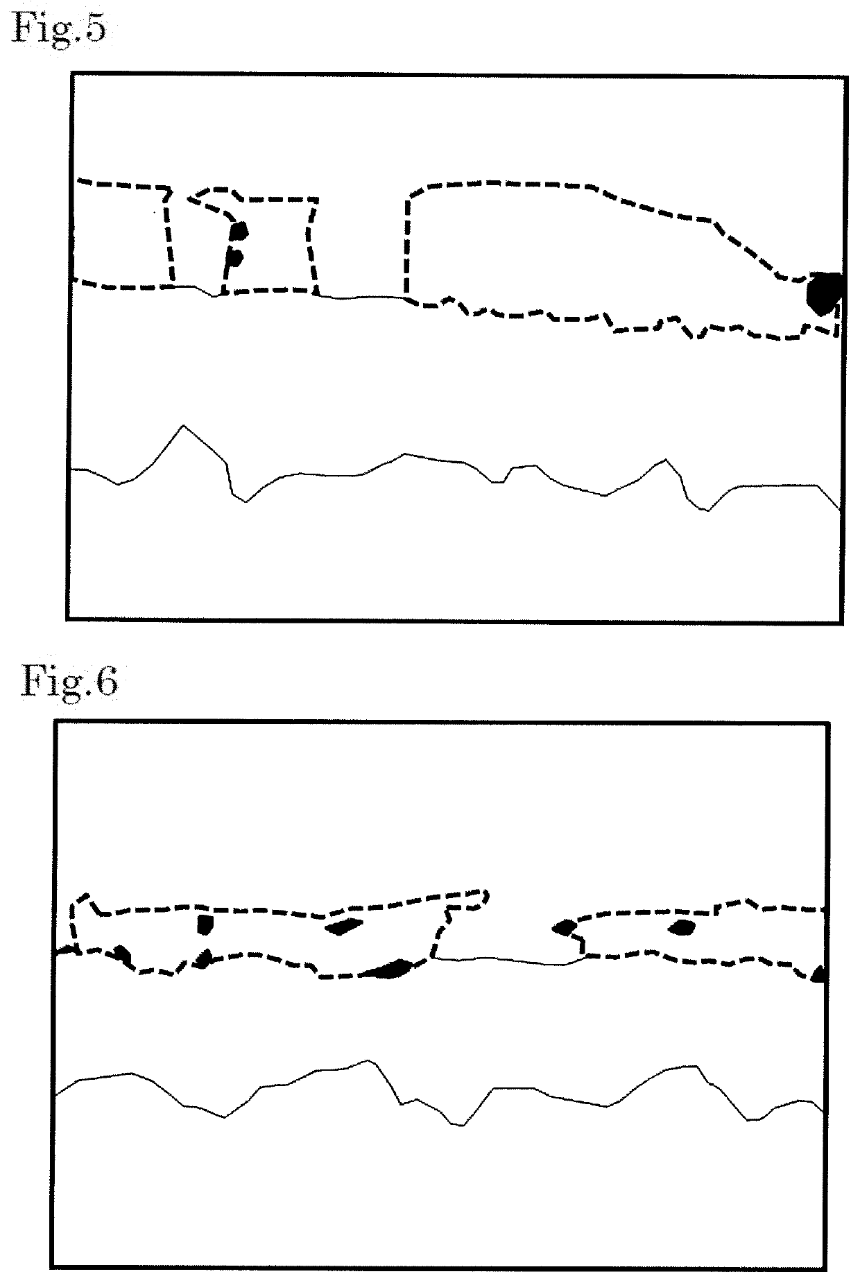
Image

Examples
example 1
[0351]The following steps (1) to (7) were carried out sequentially to prepare a cell.
[0352](1) Etching and Cleaning of FTO Substrate
[0353]A part of a glass substrate with 25 mm square fluorine doped tin oxide (FTO) (manufactured by Asahi Glass Fabritec Corporation, 25×25×1.8 mm, hereinafter referred to as FTO substrate) was etched with Zn powder and a 2 mol / L hydrochloric acid aqueous solution. Ultrasonic cleaning was carried out for 10 minutes sequentially with 1 mass % neutral detergent, acetone, 2-propanol (IPA), and ion exchanged water.
[0354](2) Ozone Cleaning
[0355]Ozone cleaning of the FTO substrate was performed immediately before the compact TiO2 layer forming step. With the FTO side facing up, the substrate was placed in an ozone generator (ozone cleaner PC-450 UV, manufactured by Meiwafosis Co., Ltd.) and irradiated with UV for 30 minutes.
[0356](3) Formation of Compact TiO2 Layer (Blocking Layer)
[0357]Bis(2,4-pentanedionato)bis(2-propanolato) titanium (IV) (4.04 g, 75% IPA ...
example 2
[0367]In (5) Formation of Light Absorption Layer of Example 1, a light absorption layer was formed in the same manner as in Example 1 to prepare a cell, except that toluene as the poor solvent was not added dropwise.
PUM
| Property | Measurement | Unit |
|---|---|---|
| porosity | aaaaa | aaaaa |
| band gap energy | aaaaa | aaaaa |
| band gap energy | aaaaa | aaaaa |
Abstract
Description
Claims
Application Information