Eureka AIR delivers breakthrough ideas for toughest innovation challenges, trusted by R&D personnel around the world.

Preparation of semiconductor substrates

a technology of indium phosphide and semiconductor substrate, which is applied in the direction of single crystal growth, electrical equipment, chemistry apparatus and processes, etc., can solve the problems of reducing device yield, affecting the purity of starting products, and achieving the purity of deposited layers using movp

Inactive Publication Date: 2000-03-14
IPG PHOTONICS CORP
View PDF8 Cites 11 Cited by
  • Summary
  • Abstract
  • Description
  • Claims
  • Application Information

AI Technical Summary

Benefits of technology

The annealing step promotes any tendency for surface accumulation of impurities, for example silicon atoms, by diffusion from the bulk substrate. Also, annealing promotes impurity atom removal from the substrate surface.
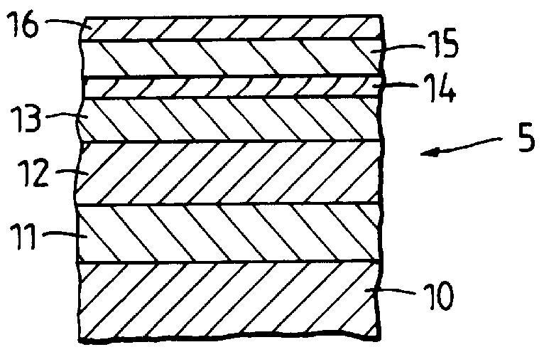
The buffer layer (or layers) provide(s) a semi-insulating barrier between the substrate and subsequently grown epitaxial layers to reduce the influence the substrate has over the nature and performance of the subsequently grown epitaxial layers.
It has been shown that iron atoms cancel the affects of n-type carriers, in effect forming `carrier traps`, and that the higher the iron concentration, the greater the insulating properties of the iron doped InP or AlInAs [3].
Other dopants, for example chromium, have been seen to act as p-type carrier traps in InP and GaAs. In general, for a dopant to act as an effective carrier trap, it is a requirement that it sits as closely as possible to the centre of the band-gap of the base material in which it is doped. Then, the dopant, and hence any trapped carriers, are as far away as possible from both the valance and conduction bands of the base material making carrier escape through thermal or electrical excitation difficult. As a result, the doped base material increases greatly in resistivity. Obviously, a dopant is selected for its ability to act either as a p-type carrier trap or as an n-type carrier trap in dependence on the type of conduction, for example due to the presence of impurities, exhibited by the base material.
The inventors have shown that a combination of annealing and a subsequently grown semi-insulating buffer layer is an effective method of greatly reducing the effects of conducting interfacial layers, in most cases. However, in some cases, for example in a case where a substrate boule proves to be particularly susceptible to parallel conduction mechanisms, a further step is included in the preparatory stages of a substrate to offer greater protection against the vagaries of substrate quality.
The further step is an etch step, which is carried out between the annealing step and the buffer layering step. The etch step removes any surface contaminants from the substrate, for example oxygen or oxides which may have contaminated the substrate from the atmosphere in which the boule is stored or transported, and provides a clean, flat surface on which subsequent epitaxial layers can be grown. The inventors have shown that any etching process, and indeed any etchant, for example phosphorus trichloride to etch InP, which is shown to provide non-preferential etching (i.e. polish etching), without unduly roughening the substrate surface, is suitable for the etching step. The inventors have also shown that gas-etching provides better results than wet-etching because gas-etching is carried out in-situ, providing exclusion of impurities that may re-contaminate the surface of the substrate. Preferably, no more than about 1um (that is to say, the first few monolayers) of surface substrate is removed to provide a substrate surface of the required cleanliness.

Problems solved by technology

The achievable purity of deposited layers using MOVPE is potentially very high but can be affected by the purity of the starting products.
As long as the starting products are not totally pure, device manufacturers have to take steps to avoid or counter the unpredictable effects that the impurities have on manufacturing processes, or suffer from reduced device yield.
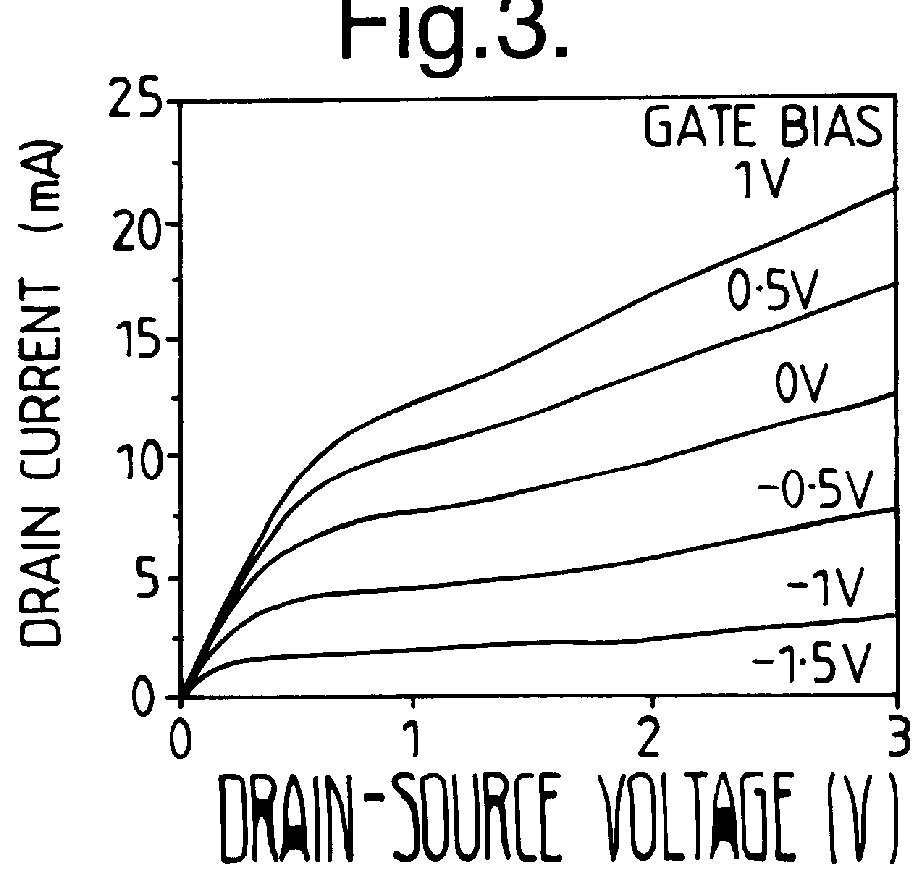
This phenomenon presents a particular problem to InP based field effect transistors (FETs) grown on Fe-doped InP substrates because it prevents pinch-off by providing a parallel conduction path that cannot be controlled by gate voltage.
This also raises output conductance, device-to-device leakage and can add a parasitic capacitance affecting high frequency performance.
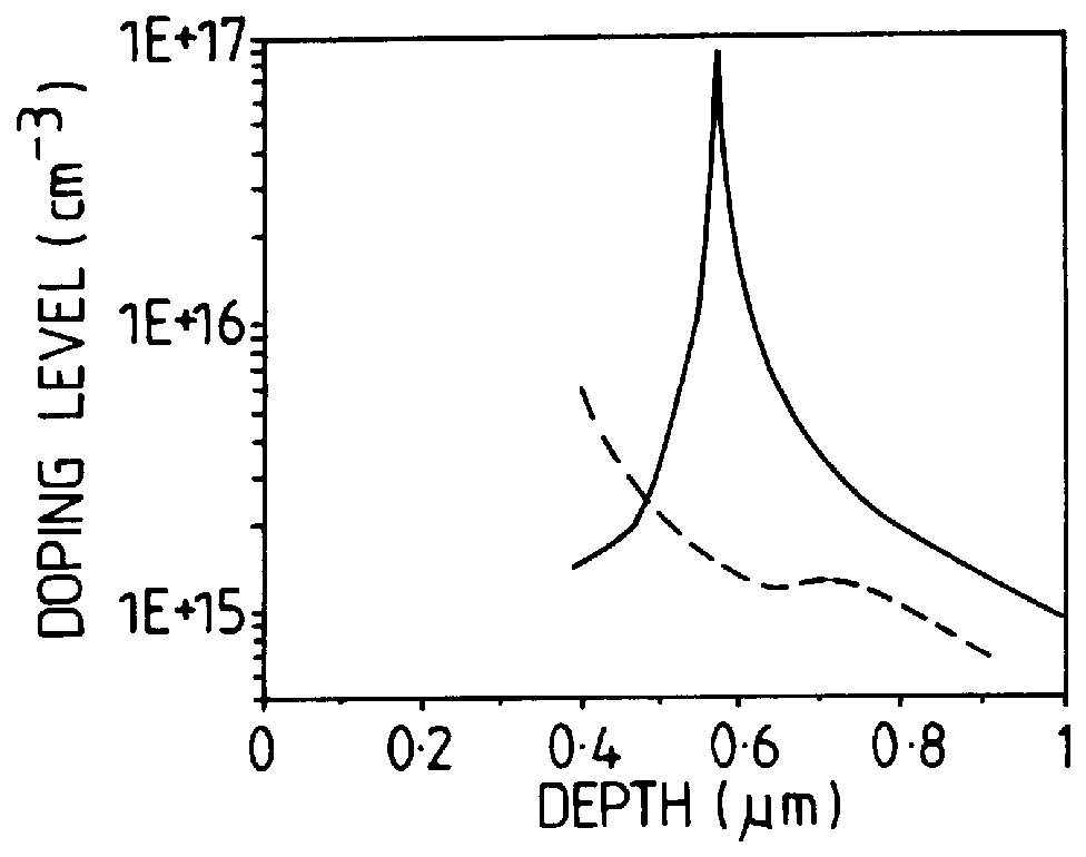
Even when below detection limits in grown layers, this is another potential source of surface contamination during wafer heat-up.
In practice, it is quite likely that several of these mechanisms may contribute to contamination simultaneously, varying in degree of severity depending on factors such as the substrate batch or manufacturer, its handling and preparation procedure, chemical batches and the history of the growth kit.
The significance of the accumulated silicon greatly increases as device complexity increases, since fabrication times increase giving the silicon more time to accumulate.
Although the existence of parallel conduction mechanisms has been recognised for at least 10 years, and more recently the causes of the mechanisms, for example n-type conduction by silicon atoms, have been isolated, surprisingly, none of the proposed methods of overcoming or countering the effects of the mechanisms have proved entirely satisfactory.
However, it has been shown that doping an InP layer with iron reduces n-type conduction in the InP.
Then, the dopant, and hence any trapped carriers, are as far away as possible from both the valance and conduction bands of the base material making carrier escape through thermal or electrical excitation difficult.

Method used


Image

  • Preparation of semiconductor substrates
  • Preparation of semiconductor substrates
  • Preparation of semiconductor substrates

Examples


Embodiment Construction

An iron-doped InP substrate was prepared for subsequent epitaxial HFET device growth as follows.

The iron-doped InP substrate was installed in an atmospheric pressure MOVPE reactor. For the annealing stage, the substrate was heated to a temperature of around 750.degree. C., in the reactor, in an atmosphere of phosphine and highly pure hydrogen.

At around 400.degree. C. the surface of an InP substrate becomes unstable unless phosphine or a similar gas is present in the atmosphere to stabilise the surface.

Typically, therefore, a phosphine flow should be present during the whole substrate heating process, or at least from around 400.degree. C. upwards.

The rate of impurity silicon atom removal from a substrate due to the annealing step has been reported to be proportional to the heating time and substrate temperature [2].

The substrate was annealed at 750.degree. C. for 30 minutes with a phosphine flow of 46 sccm (standard cubic centimetres per minute), to provide a partial overpressure of...


PUM


Abstract

An indium phosphate semiconductor substrate is prepared for subsequent growth of epitaxial layers to form a semiconductor device. In the preparation, the substrate is first annealed to promote any tendency for surface accumulation of impurity atoms by diffusion from the substrate and to promote impurity atom removal from the surface of the substrate. The substrate is then surface etched to remove further impurities and to provide a clean, flat surface for subsequent epitaxial layer growth. The final stage of preparation involves growing a semi-insulating buffer layer on the substrate to isolate the device epitaxial layers from the substrate.

Description

1. Field of the InventionThe present invention relates to the production of semiconductor devices and in particular to the preparation of indium phosphide semiconductor substrates for use in the production of semiconductor devices using MOVPE techniques.2. Related ArtMOVPE (Metal Organic Vapour Phase Epitaxy) is commonly used to grow a wide variety of semiconductor devices comprising multiple layers which require precise material composition and thickness. In some materials systems, virtually monolayer control can be achieved using MOVPE when switching from one compound to another which in some cases is essential for accurate, repeatable device fabrication. The achievable purity of deposited layers using MOVPE is potentially very high but can be affected by the purity of the starting products. As long as the starting products are not totally pure, device manufacturers have to take steps to avoid or counter the unpredictable effects that the impurities have on manufacturing processes...

Claims


Application Information

Patent Timeline
IPC IPC(8): H01L21/20H01L21/02
CPCH01L21/02392H01L21/02461H01L21/02463H01L21/02505H01L21/02543H01L21/02546H01L21/02581H01L21/02658
Inventor SPURDENS, PAUL C.SALTER, MARK A.HARLOW, MICHAEL J.NEWSON, DAVID J.
Owner IPG PHOTONICS CORP
Why Eureka
Eureka Blog
Learn More