Method of crystal growth of compound semiconductor, compound semiconductor device and method of manufacturing the device

a compound semiconductor and crystal growth technology, applied in the direction of crystal growth process, chemical apparatus and processes, pulling from melt, etc., can solve the problems of inability to produce optical devices with light-emitting wavelengths longer than gaas, inability to produce optical devices with gaas light-emitting wavelengths, and inability to achieve mass-productivity and cost. the effect of cost reduction

Inactive Publication Date: 2000-11-21
SUMITOMO ELECTRIC IND LTD
View PDF7 Cites 49 Cited by
  • Summary
  • Abstract
  • Description
  • Claims
  • Application Information

AI Technical Summary

Problems solved by technology

When this material is combined with other materials to form a multi-layer structure, an optical device having a light-emitting wavelength longer than that of GaAs can be produced, which has hitherto been impossible.
The InP substrate, however, is inferior to the GaAs substrate both in the aspects of mass-productivity and cost.
The lasers formed on such substrates are also inferior with regard to their mass-productivity and cost.
Further, the amount of source gas supplied increases in either case in which the growth temperature is raised or in which the amount of arsine supplied is increased, inducing the need to consider the problems of the exhaust gas processing and environmental pollution.
The growth of a quartenary GaInNAs-type compound semiconductor crystal, however, involves a problem not found in a ternary GaAsN-type compound semiconductor, as will be described below.
A similar problem is perceived in relation to the ternary GaInN-type compound semiconductor crystal which has the potential as a material for a blue laser device.
In this latter case, it is observed that In is less easily incorporated into the crystal since the only group V element forming the crystal is N. This problem, however, is all together a different kind of a problem from that of the N incorporation described above.
As described above, however, arsine used as the arsenic-containing group V source material has a poor decomposition efficiency.
Therefore, decrease in the amount of arsine supplied may possibly lead to degradation in the crystal characteristic.
On the other hand, lowering the growth temperature of the crystal similarly retards decomposition of arsine, leading to the degradation of the crystal characteristic.
It has been found that the optical characteristic deteriorates when the concentration of nitrogen is increased.
The presence of defects or impurities in the crystal obstructs luminescence, causing the weakening of the intensity.
Thus, when a thin film crystal having poor optical and electrical characteristics is used as the light-emitting device described above, the device undergoes a significant deterioration in its performance characteristic and reliability.
In the case in which such a thin film crystal is used as a light-receiving device, its light-receiving sensitivity becomes so low that weak light cannot be detected.
In addition, in the light-emitting device, the intensity of the emitted light becomes weak.
Further, particularly in a semiconductor laser, continuous lasing operation becomes impossible.
In both the cases of the light-emitting or light-receiving device and the electrical device, the device may not electrically operate if a layer having a high resistivity exists in the multi-layer film.
As a result, there is a problem of hydrogen being incorporated into the thin film crystal.
The characteristic of a nitrogen-containing group V source material crystal, however, may deteriorate as the source material molar supply ratio becomes greater than 10.
In addition, since Ga.sub.1-x In.sub.x N.sub.y As.sub.1-y and GaN.sub.y As.sub.1-y are compound crystal semiconductors composed of elements having atomic radii which vary greatly from one another, it is extremely difficult to obtain a crystal of a uniform composition.
It is therefore difficult to form a good quality crystal.
This is a problem originating in the combination of the material being used.

Method used


Image

  • Method of crystal growth of compound semiconductor, compound semiconductor device and method of manufacturing the device
  • Method of crystal growth of compound semiconductor, compound semiconductor device and method of manufacturing the device
  • Method of crystal growth of compound semiconductor, compound semiconductor device and method of manufacturing the device

Examples


second embodiment

As seen from FIGS. 7 and 8 described with reference to the second embodiment, when the growth was effected at 600.degree. C. with GaNAs, the nitrogen concentration was varied in the range of 1.8.times.10.sup.19 to 1.5.times.10.sup.21, while the hydrogen concentration showed a low concentration in the range of 2.9.times.10.sup.17 to 1.1.times.10.sup.18. The intensity for InGaAsP being 20, the luminescence intensity of GaNAs was 2.3 to 2.6, which implies that the luminescence intensity sufficient for practical use was obtained at all nitrogen concentration levels.

On the other hand, at 530.degree. C., there is a strong correlation between the concentration of hydrogen and the luminescence intensity. With a low concentration of nitrogen in the range of 1.8.times.10.sup.19 to 1.0.times.10.sup.20, the -hydrogen concentration was in the range of 3.8.times.10.sup.17 to 2.7.times.10.sup.18, and the luminescence intensity was in the range of 1.8 to 14. With a high concentration of nitrogen in...

sixth example

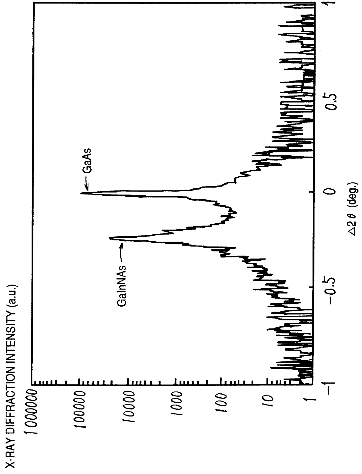
Using the growth method described with reference to the first example, at the temperature of 530.degree. C., the concentration of hydrogen within the crystals for either the cases of Ga.sub.1-x In.sub.x N.sub.y As.sub.1-y or GaN.sub.y As.sub.1-y becomes 5.times.10.sup.18 atoms / cm.sup.3 or more (see FIGS. 7 and 8).

After growing the structure described in the fifth example under these conditions, the structure was reheated under the following conditions. Thereafter, the optical and electrical characteristics were measured.

In this heat treatment, an SiN film was grown to the thickness of 100 nm by plasma CVD (Chemical Vapor Deposition) to prevent the evaporation of As from the surface. The SiN film was removed by a 5% hydrofluoric acid after the heat treatment.

The above structure was heat treated in a hydrogen atmosphere at 76 Torr. A quartz heating furnace was used for the heat treatment. The example in which a GaN.sub.0.012 As.sub.0.988 sample was heat treated will be described below...

seventh example

This example relates to heat treatment within a growth furnace.

Using the growth method described with reference to the fifth example, at the growth temperature of 530.degree. C. as in the sixth example, the GaN.sub.0.012 As.sub.0.988 and Ga.sub.0.9 In.sub.0.1 N.sub.0.035 As.sub.0.965 DH structures were grown. A sufficient luminescence characteristic is not obtained without heat treatment. Thus, heat treatment was performed after the growth of the DH structures without lowering the temperature.

FIG. 13 shows the temperature profile of the device structure subjected to reheating after the growth.

FIG. 14 shows the observed changes in the temperature and the time for heat treatment and in the gas supply when the device structure is heat treated after the growth without experiencing a decrease in temperature. When the DH structure was grown, hydrogen, TMG and TBAs gases were supplied to the sample in order to allow the growth of the uppermost GaAs layer. In order to prevent the desorption...


PUM


Abstract

A semiconductor layer consisting of Ga1-xInx NyAs1-y and / or GaNyAs1-y and formed by incorporating nitrogen into a group III-V mixed crystal semiconductor is provided on a GaAs substrate. The hydrogen concentration in the semiconductor is kept at 5x10¹⁸ atoms / cm3 or below.

Description

1. Field of the InventionThe present invention relates to a method of crystal growth of a compound semiconductor, and more specifically to a method of crystal growth of a GaInNAs-type compound semiconductor by a vapor phase growth method. The invention also relates to a compound semiconductor device having as a part of the device a Ga.sub.1-x In.sub.x N.sub.y As.sub.1-y or GaN.sub.y As.sub.1-y crystal thin film. The invention further relates to a method of manufacturing such a compound semiconductor device.2. Description of the Background ArtFirst of all, the background art relating to the compound semiconductor device using GaInNAs will be described.As mentioned earlier, in recent years, a group III-V mixed crystal semiconductor containing nitrogen as a group V element has received much attention as a novel semiconductor material. With this material, through appropriate selection of the concentrations of nitrogen and component elements, epitaxial growth without misfit dislocation o...

Claims


Application Information

Patent Timeline
Patent Type & Authority Patents(United States)
IPC IPC(8): H01L31/12H01L31/0264H01L31/0304H01L31/18H01L33/00H01L33/32
CPCH01L31/03046H01L31/125H01L31/1844Y02E10/544H01L33/0075H01L33/32
Inventor TANAKA, SOMOTO, AKIHIROTANABE, TATSUYAIKOMA, NOBUYUKI
Owner SUMITOMO ELECTRIC IND LTD
Why Eureka
Try Eureka