Virtual shutter method and apparatus for preventing damage to gallium arsenide substrates during processing

a shutter method and gallium arsenide technology, applied in the direction of electrolysis components, vacuum evaporation coatings, coatings, etc., can solve the problems of n-type gaas surfaces, adversely affecting device formation, and damage to the surface of gaas substrates

Inactive Publication Date: 2000-12-05
BECHTEL BWXT IDAHO +1
View PDF6 Cites 17 Cited by
  • Summary
  • Abstract
  • Description
  • Claims
  • Application Information

AI Technical Summary

Problems solved by technology

Conventional processes for depositing refractory metals have the potential of causing damage to GaAs substrates that adversely affects devices being formed thereon that have features having such decreased dimensions.
Certain stages of a PVD process, such as the plasma ignition stage, can subject the surface of a GaAs substrate to damage.
For example, implanted n-type GaAs surfaces that are exposed directly to the plasma ignition stage in a DC magnetron PVD system can incur damage from impinging secondary electrons, from ions, and from reflected fast neutral atoms that are produced during plasma ignition.
Although DC magnetron sputtering produces relatively low damage to GaAs substrates, the performance of some devices such as field effect transistors (FETs) can be affected by damage resulting from DC ...

Method used


Image

  • Virtual shutter method and apparatus for preventing damage to gallium arsenide substrates during processing
  • Virtual shutter method and apparatus for preventing damage to gallium arsenide substrates during processing
  • Virtual shutter method and apparatus for preventing damage to gallium arsenide substrates during processing

Examples


Embodiment Construction

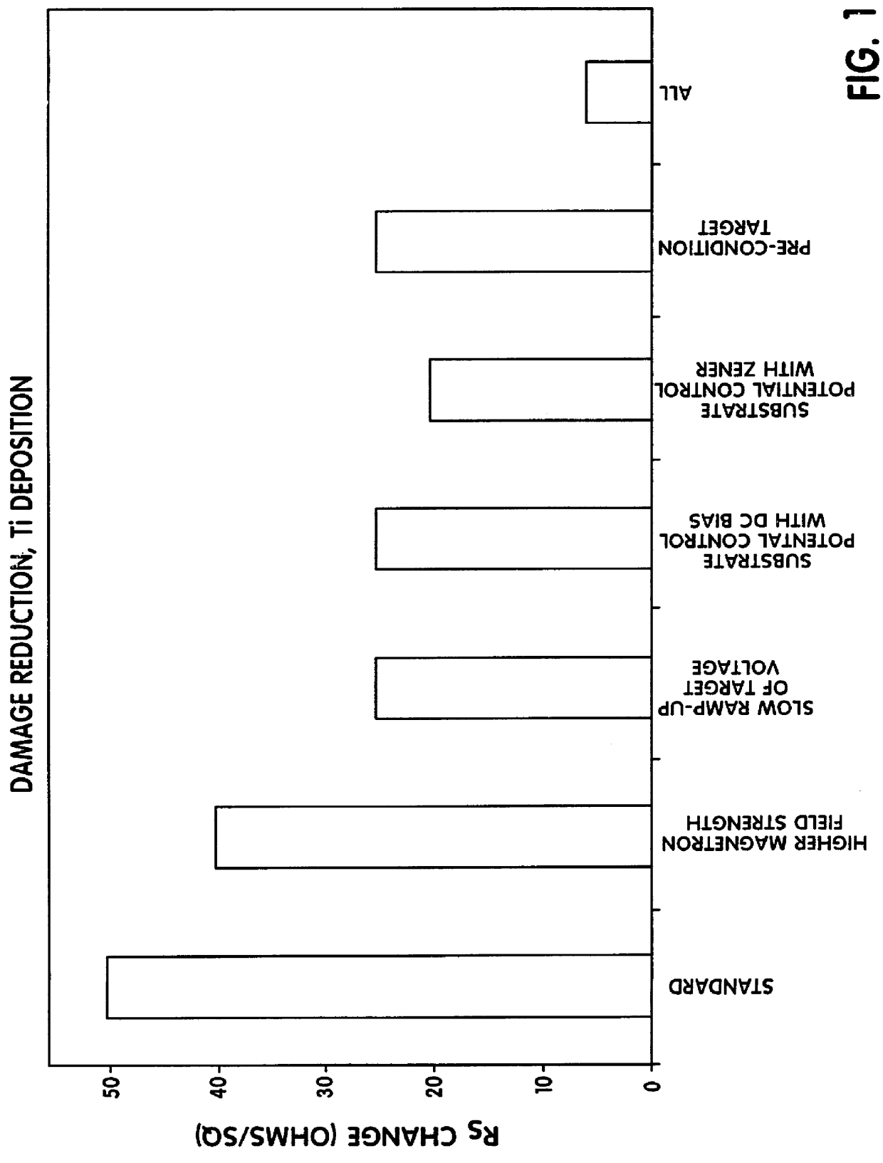
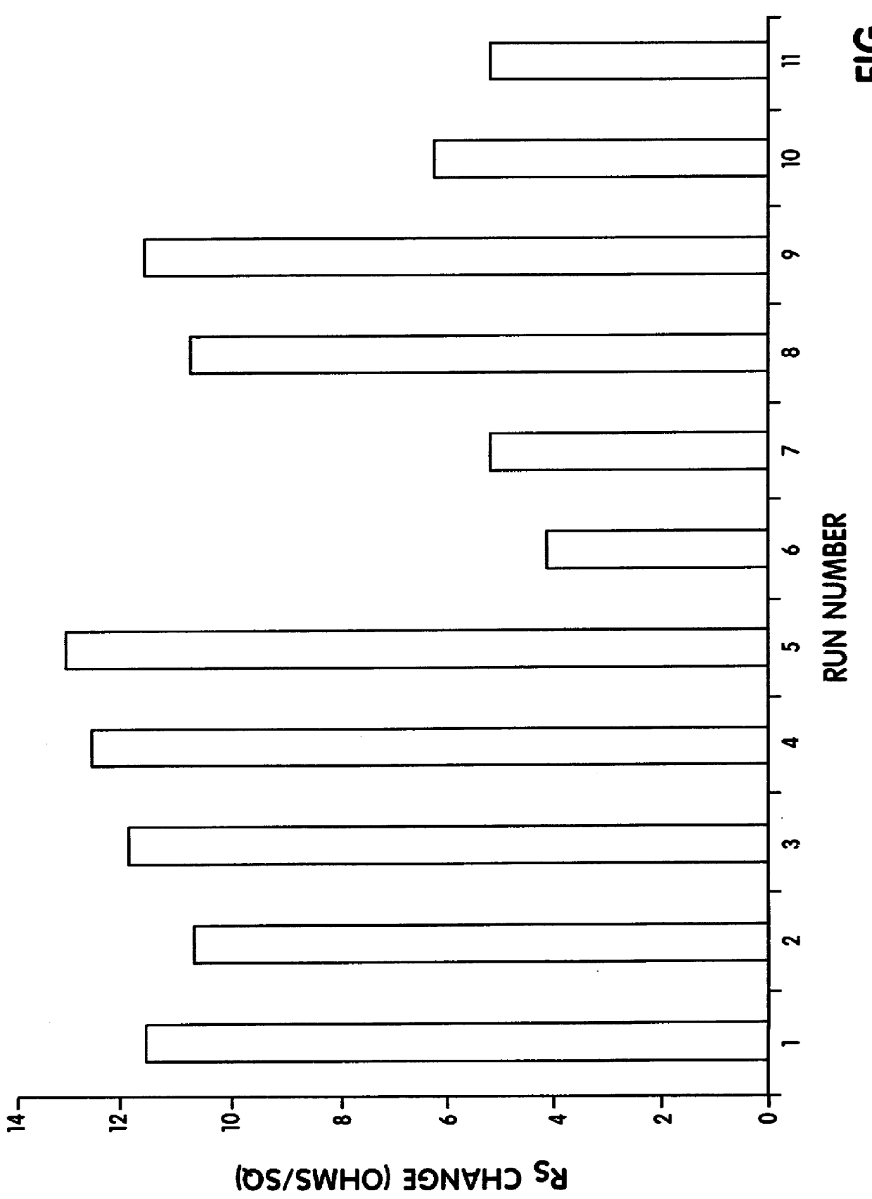
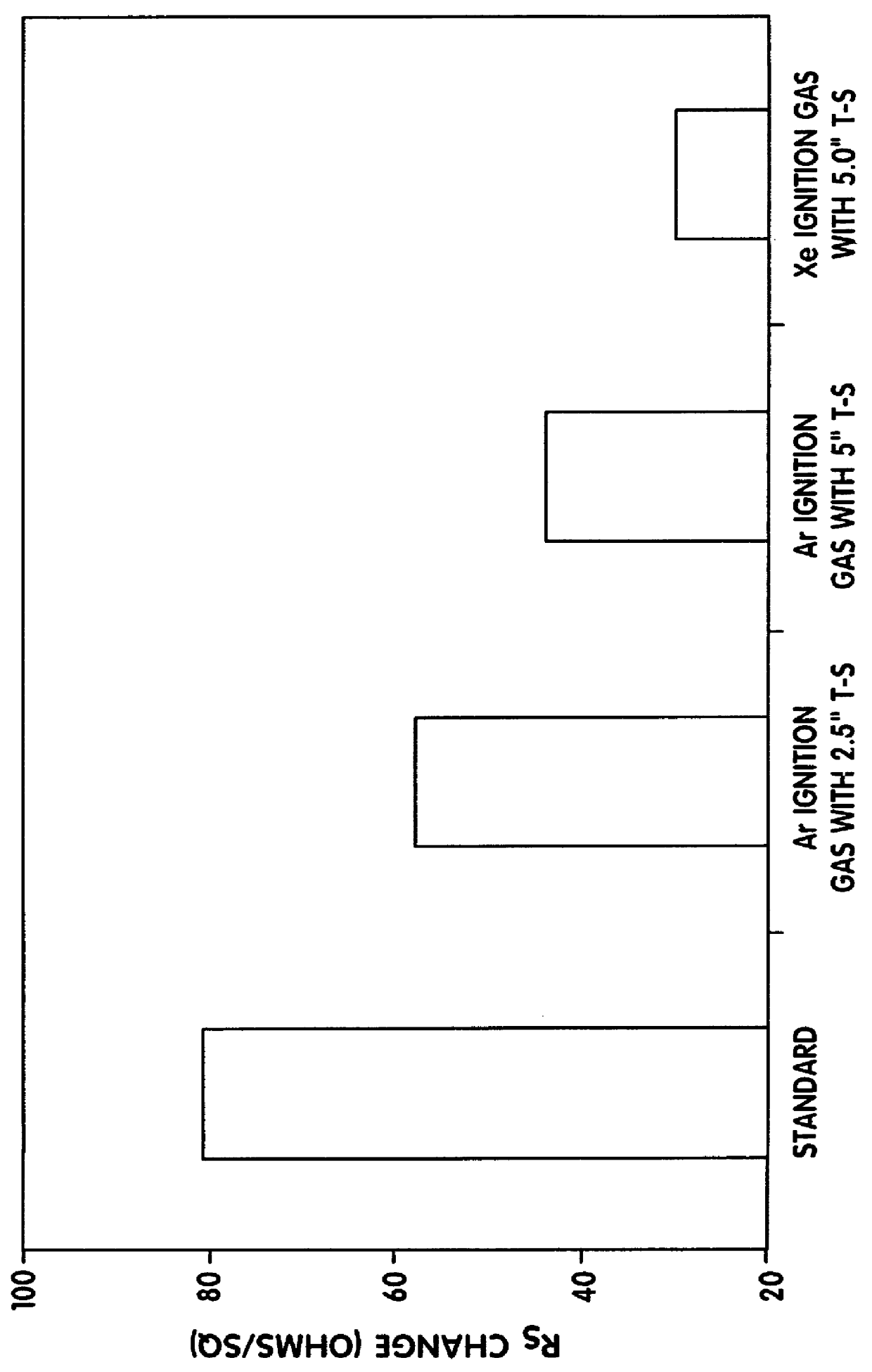
Each component of the virtual shutter concept evaluated for damage reduction has been evaluated in experiments by monitoring changes in sheet resistance (R.sub.S) on n-type GaAs substrates. In such experiments, GaAs substrates were prepared by implanting new GaAs wafers with silicon (Si), encapsulated with silicon nitride (Si.sub.3 N.sub.4), and the implant was activated using a rapid thermal anneal. After removing the Si.sub.3 N.sub.4, the pre-deposition R.sub.S of the n-GaAs wafers was measured using a non-contact resistivity measurement system. The n-GaAs wafer was then used to test various plasma ignition and deposition sequences. After PVD processing, the deposited metal was chemically etched and the post-deposition R.sub.S was measured. The change in R.sub.S was calculated by using the difference of the average post and predeposition values. The average value comprised fifty-four measurement points per wafer.

The magnitude of the R.sub.S change is a strong indicator of FET devi...


PUM

PropertyMeasurementUnit
Timeaaaaaaaaaa
Timeaaaaaaaaaa
Lengthaaaaaaaaaa

Abstract

Damage to a gallium arsenide substrate during plasma ignition for PVD processing is avoided by a virtual shutter, which provides the functions without the disadvantages of a mechanical shutter to minimize the density of high energy particles created during plasma ignition from reaching the GaAs substrate. A plasma ignition process sequence uses a high pressure gas ignition gas burst in combination with the control of other parameters, such as (a) varying the plasma ignition gas composition to include xenon, krypton or fluorinated molecular gases, (b) varying target-to-substrate distance to at least double the distance during plasma ignition, (c) increasing the magnetron magnetic field strength either permanently or during plasma ignition to about 400 Gauss, (d) preconditioning the target by sputtering whenever the system has been idle for several minutes, (e) adjusting the power supply power ramping to the target over 5-6 seconds or more, and/or (f) using a simple electric circuit to drain charge build up on the GaAs substrate.

Description

This invention relates to the physical vapor deposition and, more particularly, to a method and apparatus for depositing onto substrates, particularly substrates formed of gallium arsenide, coatings, particularly refractory metal coatings, by physical vapor deposition.BACKGROUND OR THE INVENTIONIn the manufacture of semiconductors that are formed using gallium arsenide (GaAs) wafers, device feature dimensions such as integrated circuit implant depth and gate width continue to decrease. To form such features, deposition of refractory metals is typically employed. Conventional processes for depositing refractory metals have the potential of causing damage to GaAs substrates that adversely affects devices being formed thereon that have features having such decreased dimensions. Physical vapor deposition (PVD) has become recognized as a process useful to deposit refractory metals to form sub-micron sized features such as, for example, ohmic and Shottky contacts, on GaAs wafers.Certain s...

Claims


Application Information

Patent Timeline
IPC IPC(8): C23C14/35C23C14/54C23C14/34
CPCC23C14/54C23C14/35
Inventor SMOLANOFF, JASONCALDWELL, DOUGREYNOLDS, GLYN
Owner BECHTEL BWXT IDAHO
Why Eureka
Try Eureka