Method for fabricating a semiconductor device

a semiconductor and device technology, applied in the direction of semiconductor devices, electrical appliances, transistors, etc., can solve the problems of difficult to obtain the required crystallinity, difficult to obtain a good annealing effect across the wide area, and the irradiation of laser light is apt to become unstabl

Inactive Publication Date: 2001-01-30
SEMICON ENERGY LAB CO LTD
View PDF126 Cites 162 Cited by
  • Summary
  • Abstract
  • Description
  • Claims
  • Application Information

AI Technical Summary

Problems solved by technology

However, it has been difficult to obtain a required crystallinity across the wide area through the heat treatment because it may cause nonuniformity in the crystallization.
Further, although it is possible to obtain the high crystallinity partly by irradiating laser light, it is difficult to obtain a good annealing effect across the wide area.
In particular, the irradiation of the laser light is apt to become unstable under the conditions needed for obtaining the good crystallinity.
However, it is difficult to obtain a crystalline silicon film having high crystallinity and homogeneity across a wide area which is required for an active matrix type liquid crystal display.
Further, because the metal elemen...

Method used


Image

  • Method for fabricating a semiconductor device
  • Method for fabricating a semiconductor device
  • Method for fabricating a semiconductor device

Examples


second embodiment

The present embodiment relates to a case when Cu is used as the metal element which promotes the crystallization of silicon in the arrangement shown in the first embodiment. In this case, cupric acetate [Cu(CH.sub.3 COO).sub.2 ] or cupricchloride (CuCl.sub.2 2H.sub.2 O) may be used as the solution for introducing Cu.

third embodiment

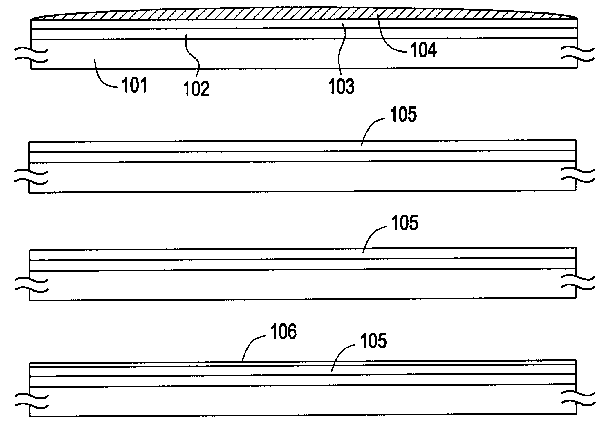
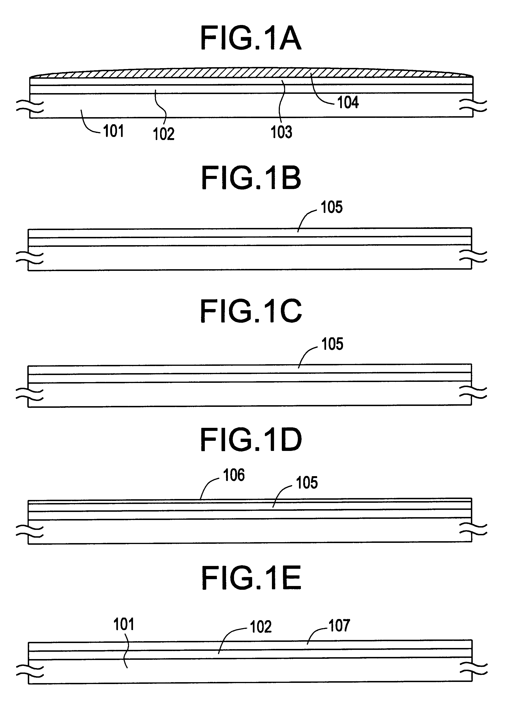
The present embodiment relates to a case of growing crystal in the form different from that in the first embodiment. That is, the present embodiment relates to a method of growing the crystal in a direction parallel to the substrate, i.e. a method called lateral growth, by utilizing the metal element which promotes crystallization of silicon.

FIG. 2 shows the fabrication process according to the present embodiment. At first, a silicon oxide nitride film is formed as an underlying film 202 in a thickness of 3000 angstrom on the Corning 1737 glass substrate (or a quartz substrate) 201.

Next, an amorphous silicon film 203 which is the starting film for a crystalline silicon film is formed in a thickness of 600 angstrom by low pressure thermal CVD. The thickness of the amorphous silicon film is preferable to be less than 2000 angstrom as described before.

It is noted that plasma CVD may be used instead of the low pressure thermal CVD.

Next, a silicon oxide film not shown is formed in a thic...

fourth embodiment

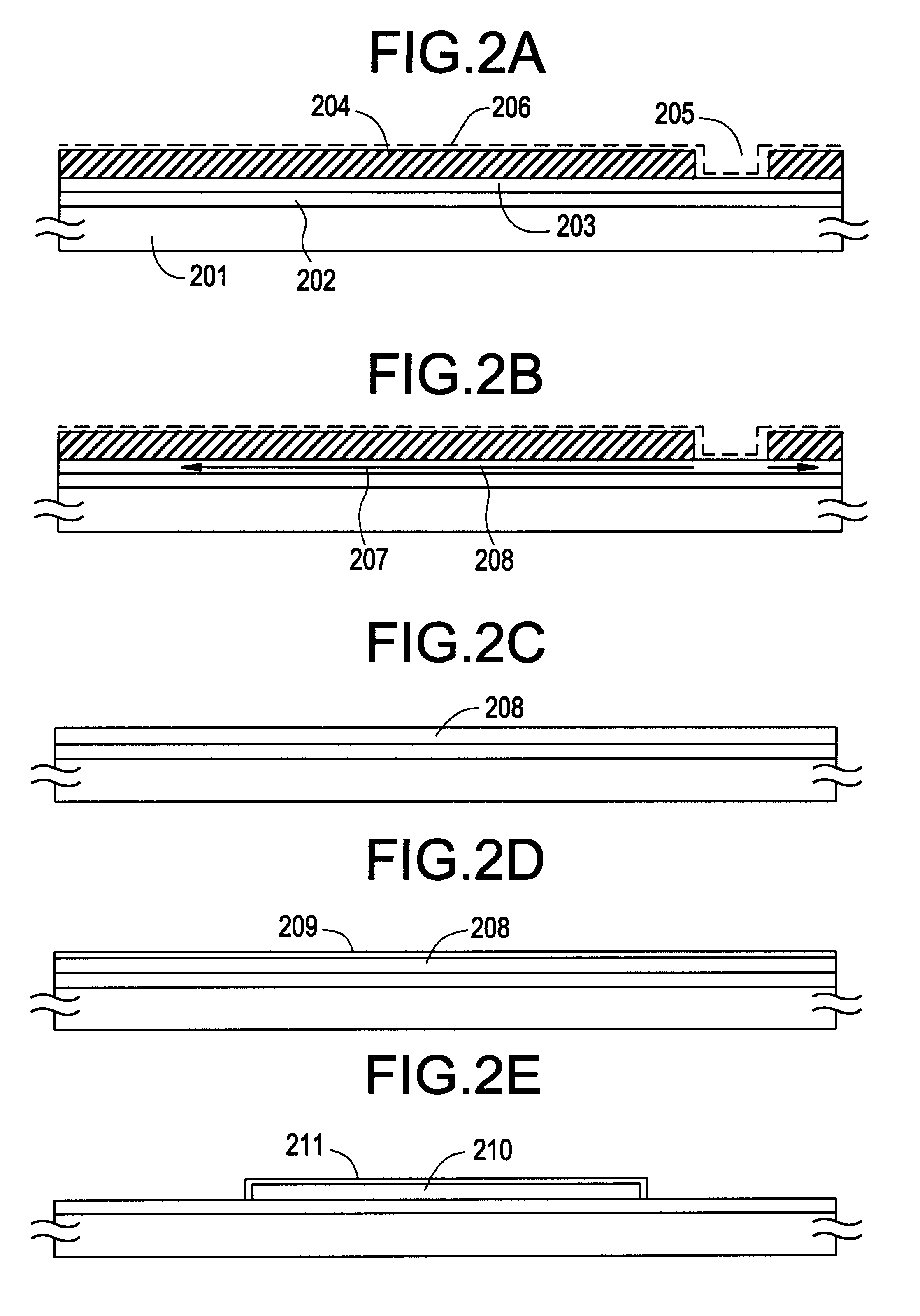
The present embodiment relates to a case of fabricating a thin film transistor disposed in a pixel region of an active matrix type liquid crystal display or an active matrix type EL display by utilizing the invention disclosed in the present specification.

FIG. 3 shows the fabrication process according to the present embodiment. At first, the crystalline silicon film is formed on the glass substrate through the process shown in the first or the third embodiment. When the crystalline silicon film is obtained by the arrangement shown in the first embodiment, it is patterned to obtain the state shown in FIG. 3A.

In the state shown in FIG. 3A, the reference numeral 301 denotes a glass substrate, 302 an underlying film, and 303 an active layer formed of the crystalline silicon film. After obtaining the state shown in FIG. 3A, a plasma treatment is performed within a reduced pressure atmosphere in which oxygen and hydrogen are mixed. The plasma is generated by high-frequency discharge.

Organ...


PUM


Abstract

Concentration of metal element which promotes crystallization of silicon and which exists within a crystalline silicon film obtained by utilizing the metal element is reduced. A first heat treatment for crystallization is performed after introducing nickel to an amorphous silicon film 103. Then, laser light is irradiated to diffuse nickel element which is concentrated locally. After that, another heat treatment is performed within an oxidizing atmosphere at a temperature higher than that of the previous heat treatment. At this time, HCl or the like is added to the atmosphere. A thermal oxide film 106 is formed in this step. At this time, gettering of the nickel element into the thermal oxide film 106 takes place. Then, the thermal oxide film 106 is removed. Thereby, a crystalline silicon film 107 having low concentration of the metal element and a high crystallinity can be obtained.

Description

The present invention relates to a semiconductor device typified by a thin film transistor and to a fabrication method thereof. Specifically, the present invention relates to a semiconductor device using a crystalline silicon thin film formed on a glass substrate or a quartz substrate and to a fabrication method thereof.DESCRIPTION OF RELATED ARTHitherto, there has been known a thin film transistor using a silicon film, i.e. a technology for forming the thin film transistor by using the silicon film formed on a glass substrate or quartz substrate.The glass substrate or quartz substrate is used because the thin film transistor is used for an active matrix type liquid crystal display. While a thin film transistor has been formed by using an amorphous silicon film in the past, it is being tried to fabricate the thin film transistor by utilizing a silicon film having a crystallinity (referred to as "crystalline silicon film" hereinbelow) in order to enhance its performance.The thin film...

Claims


Application Information

Patent Timeline
IPC IPC(8): H01L21/70H01L21/02H01L29/66H01L21/20H01L21/336H01L27/12H01L21/322H01L29/786H01L21/84H01L29/49H01L29/40H01L21/77
CPCH01L21/2022H01L21/2026H01L21/3226H01L27/1203H01L27/1277H01L27/1296H01L29/0657H01L29/66757H01L29/66765H01L29/78621H01L29/78675H01L29/4908H01L21/02592H01L21/02686H01L21/02488H01L21/02422H01L21/02532H01L21/0242H01L21/02672H01L21/02691
Inventor YAMAZAKI, SHUNPEITERAMOTO, SATOSHIKOYAMA, JUNOGATA, YASUSHIHAYAKAWA, MASAHIKOOSAME, MITSUAKI
Owner SEMICON ENERGY LAB CO LTD
Why Eureka
Try Eureka