
Thin film forming device for forming silicon thin film having crystallinity

Inactive Publication Date: 2001-02-27
NISSIN ELECTRIC CO LTD
View PDF6 Cites 16 Cited by
  • Summary
  • Abstract
  • Description
  • Claims
  • Application Information

AI Technical Summary

Problems solved by technology

However, it is impossible to use the above glass of a low softening point in the conventional device.
Consequently, an excessively large quantity of ions are incident on the base material 10.
Therefore, growth of crystals of the thin film formed on the base material is obstructed, and damage (defect) is caused on the film, that is, it is difficult to form an excellently crystalline thin film.
Accordingly, the neutralizing action by electrons, which are incident in the negative polarity cycle, becomes insufficient.
Therefore, charge-up of the base material 10 can not be effectively suppressed.
Accordingly, irradiation of ions onto the base material 10 becomes difficult.
Therefore, crystallization of the thin film obtained by ion irradiation can not be effectively facilitated.
When the voltage exceeds 1000 V, energy of ion irradiation becomes too high, and damage is given to the thin film, and crystallization is lowered on the contrary.
Therefore, charge-up can not be effectively suppressed.
When the voltage exceeds 100 V, negative charge-up voltage becomes too high when electrons are excessively incident on the base material 10, which causes a harmful effect.

Method used


Image

  • Thin film forming device for forming silicon thin film having crystallinity
  • Thin film forming device for forming silicon thin film having crystallinity
  • Thin film forming device for forming silicon thin film having crystallinity

Examples


Embodiment Construction

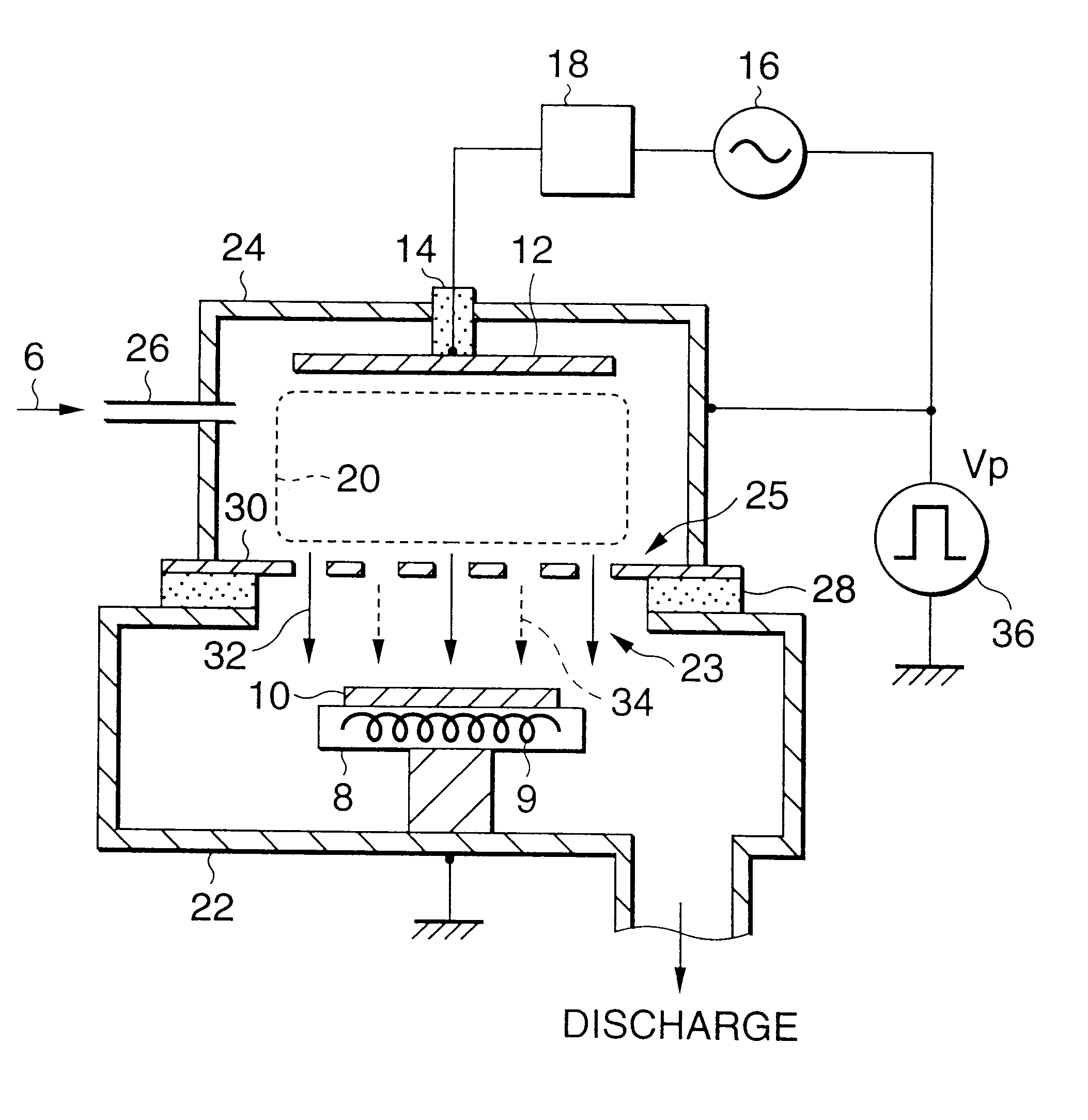
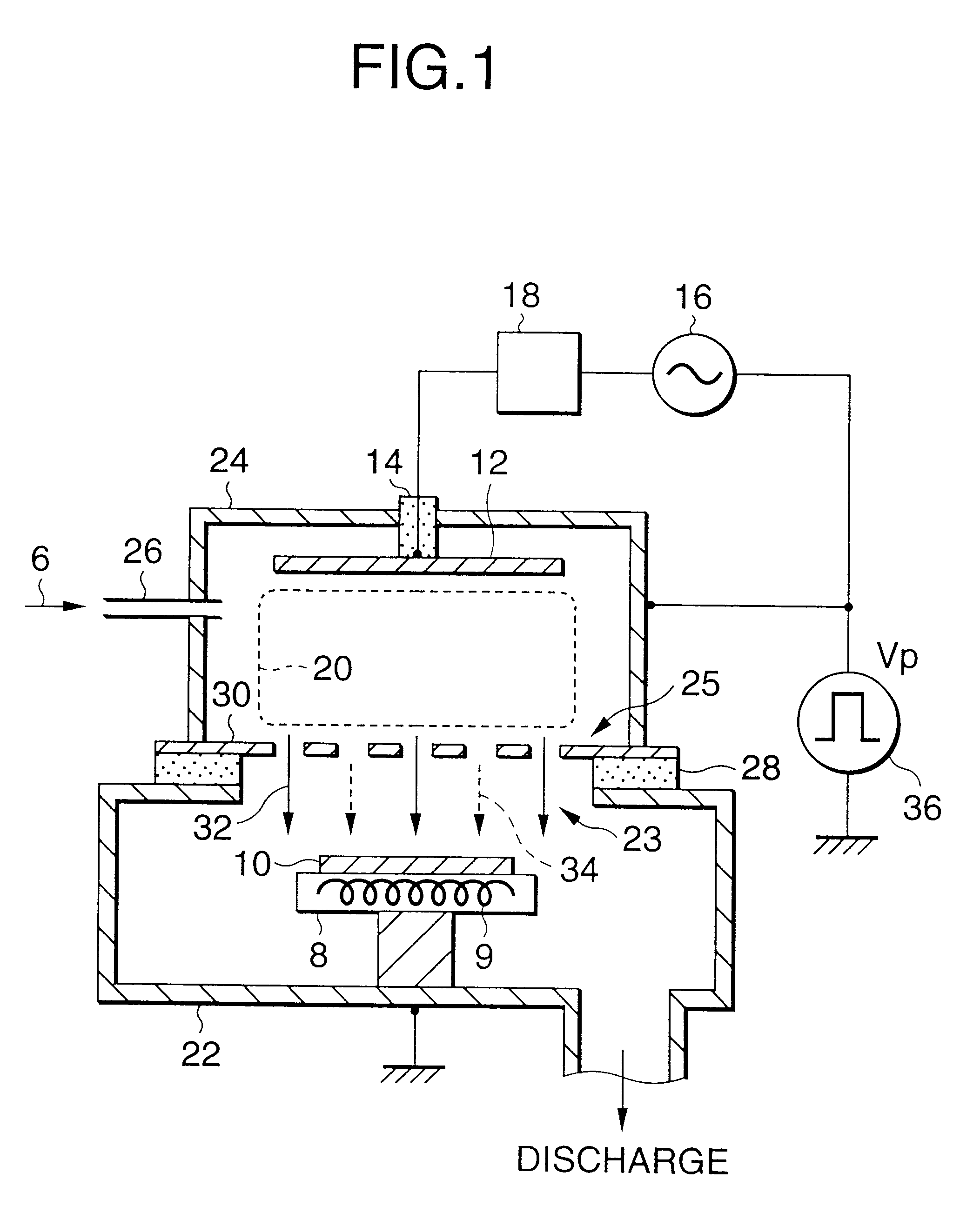
In this example, the device shown in FIG. 1 was used, and a thin film of silicon was formed on the base material 10 under the following conditions:

Frequency of high frequency electric power: 60 MHz

Introduced raw material gas: SiH.sub.4 (50%) / H.sub.2, 10 sccm

Introduced inert gas: Ar 5 sccm

Pressure in plasma chamber container: 1.times.10.sup.-4 Torr

Voltage of positive polarity portion of pulse voltage: 500 V

Voltage of negative polarity portion of pulse voltage: 100 V

Frequency of pulse voltage: 500 Hz

Duty ratio of pulse voltage: 50%

Base material: Non-alkali glass base plate or silicon base plate of face (100)

Base material temperature 400.degree. C.

Film thickness: 100 nm

As a comparative example, the conventional device shown in FIG. 5 was used, and a thin film was formed under the conditions listed above except for the impression of pulse voltage. One evaluation was conducted as follows. Concentration of hydrogen contained in a thin film of silicon formed on a silicon base plate was mea...


PUM

PropertyMeasurementUnit
Fractionaaaaaaaaaa
Angleaaaaaaaaaa
Electric potential / voltageaaaaaaaaaa

Abstract

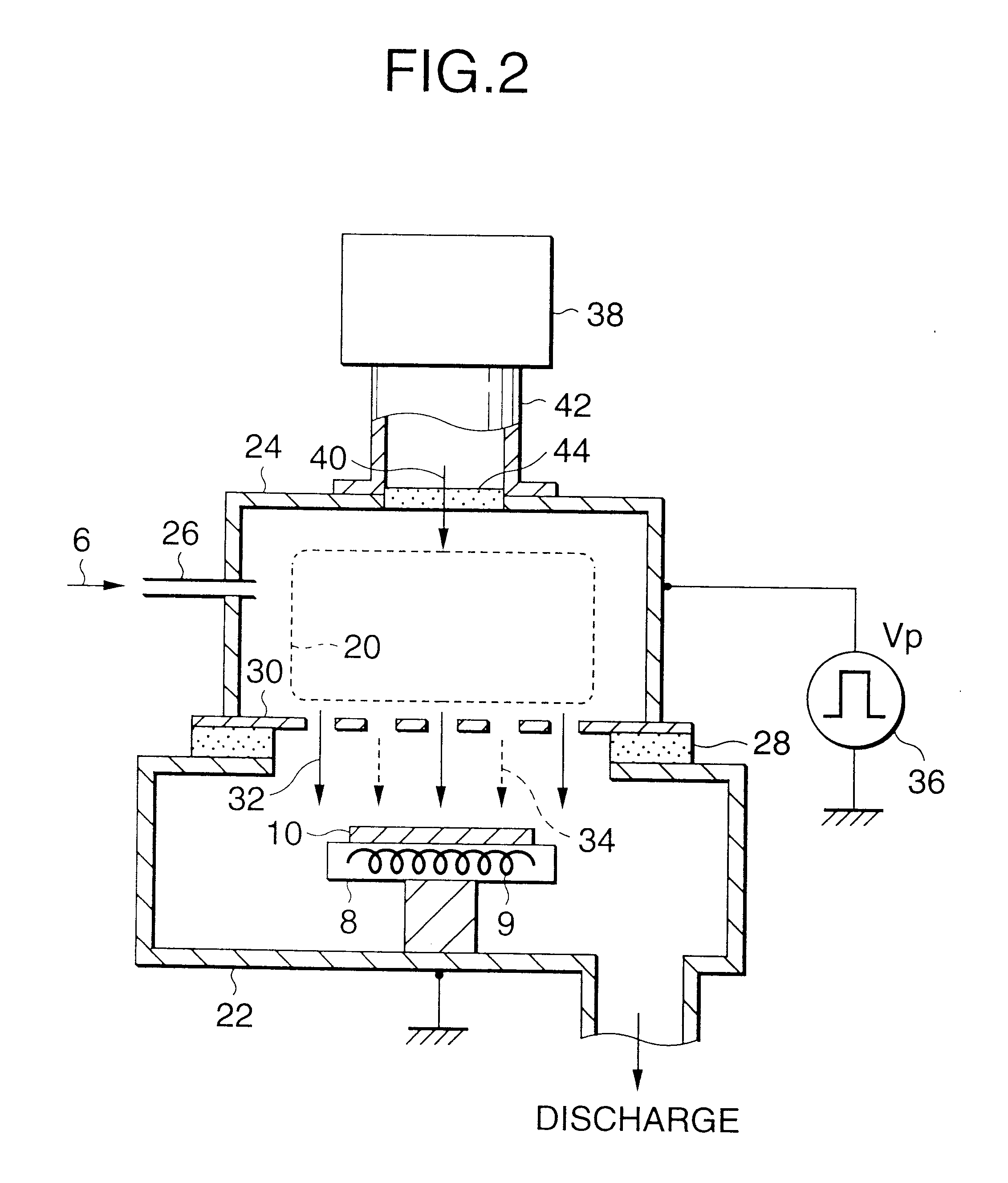
An insulating member is interposed between a film formation chamber container and a plasma chamber container. Both containers are adjacent to and communicated with each other. In the film formation chamber container, a base material holder is provided for holding the base material. Raw material gas is introduced into the plasma chamber container and ionized by high frequency electric discharge, to generate plasma. A high frequency electrode and a high frequency electric power source are provided as a plasma generating unit. There is provided a porous electrode 30, the electric potential of which is the same as that of the plasma chamber container 24, between both chambers 22, 24 to partition both chambers. A pulse electric powder source for impressing bipolar pulse voltage, in which a positive polarity portion and a negative polarity portion are alternately repeated, is provided between the base material holder and both of the plasma chamber container and the porous electrode 30, the electric potential of which is the same as that of the plasma chamber container 24.

Description

1. Filed of the InventionThe present invention relates to a thin film forming device for forming a thin film on a base material by the plasma CVD (Chemical Vapor Deposition) method. More particularly, the present invention relates to the device capable of forming an excellently crystalline thin film without heating a base material to high temperature.2. Description of the Related ArtIn order to manufacture a thin film transistor (TFT) for composing a liquid crystal display, a semiconductor integrated circuit or a solar battery, a thin crystalline film is formed on a base material, for example, a thin silicon film is formed on the base material.One of the means for forming the thin crystalline film is the plasma CVD method. According to the plasma CVD method, raw material gas is decomposed in plasma so that a thin film is formed on the base material. Therefore, the plasma CVD method is advantageous in that the base material can be kept at a relatively low temperature.FIG. 5 is a view...

Claims


Application Information

Patent Timeline
IPC IPC(8): C23C16/448C23C16/452C23C16/517C23C16/50H01J37/32C23C16/509C23C16/511C23C16/515H01L21/205H01L21/31
CPCC23C16/452C23C16/517H01J37/32091H01J37/32146
Inventor TAKAHASHI, EIJIKIRIMURA, HIROYA
Owner NISSIN ELECTRIC CO LTD
Learn More