Inductive self-soldering printed circuit board

a printed circuit board and self-soldering technology, applied in the direction of soldering apparatus, manufacturing tools, electric/magnetic/electromagnetic heating, etc., can solve the problems of requiring rework, generating rejections, increasing the cost of final products, etc., to improve the quality and reliability of manufactured products, reduce the cost of manufactured products, and reduce temperature exposure

Inactive Publication Date: 2001-05-08
TRUCCO HORACIO ANDRES
View PDF9 Cites 60 Cited by
  • Summary
  • Abstract
  • Description
  • Claims
  • Application Information

AI Technical Summary

Benefits of technology

The general objective of this invention is to provide the electronic manufacturing or electronic packaging industry with a new, safe, reliable, speedier and useful device for inductively soldering components to a PCB. Because my invention only heats the leads and pads to be joined by solder while the rest of a component (namely its casing or housing) remains relatively cold, utilization of my invention will help to reduce manufactured-product cost. For example, lower-priced components rated to tolerate much lower temperature exposure (than now required when utilizing reflow or wave solder processes) will be acceptable. My invention eliminates the need to de-moisturize certain components, for example the requirement set by the Joint Electronic Devices Engineering Council (JEDEC) to bake plastic BGAs at 125.degree. C. for 24 hours prior to reflow is eliminated. Also my invention allows to improve the quality and reliability of the manufactured product. My invention helps reduce formation of intermetallic layers inside soldered joints thus improving their robustness. My invention also induces a fast rate of solder solidification resulting in more robust soldered joints. Furthermore, my invention permits in-process and in-situ testing of soldered joints quality, thus allowing rework before final assembly is completed. My invention can solder a typical PCB up to fifty times faster than wave or reflow processes. In addition it provides for a useful de-soldering device. My invention consumes about 200 times less energy than the reflow process. My invention also allows to reduce the required manufacturing floor space.Further objectives and advantages of my invention will become apparent from a consideration of the drawings and following descriptions.

Problems solved by technology

Both processes exhibit inherit disadvantages that indeed, increase the cost of the final product, generate rejects, require rework and reduce the reliability of the final product.
The electronic manufacturing industry accepts these inherit drawbacks and shortcomings, and works around them, for lack of a more suitable soldering process.
Therefore, all electronic components must be unnecessarily temperature-overrated to tolerate or survive the harsh soldering process.
This requirement for high-temperature-exposure survival increases the cost of every component to be soldered to a PCB.
During the soldering process, thermal shock (due to a fast heating rate) can crack certain components, in particular ceramic capacitors, increasing rejects and / or requiring costly rework.
Fast heating of plastic IC packages could induce cracking when moisture absorbed inside said packages can turn into steam during a reflow soldering process causing the so called "pop-corn" effect that internally damage the IC package.
Electrolytic capacitors are extremely sensitive to high temperature exposure.
An increase in soldering process temperature can damage a PCB metal-plated through-holes or vias, by cracking their barrels due to differential thermal expansion between the PCB dielectric material and its barrels' plating metal.
Also, the difference in coefficient of thermal expansion between board and ceramic capacitors can result in significant stress at the soldered joints which may induce cracking.
Warpage, or twisting of a PCB, increases with soldering temperature.
Warpage can cause defective soldered joints because coplanarity of the mating surfaces is compromised.
In addition, defective joints result due to movement of the components from their intended soldering pads location.
This type of electrical interconnection is not as desirable as traditional soldered joints.

Method used


Image

  • Inductive self-soldering printed circuit board
  • Inductive self-soldering printed circuit board
  • Inductive self-soldering printed circuit board

Examples


Embodiment Construction

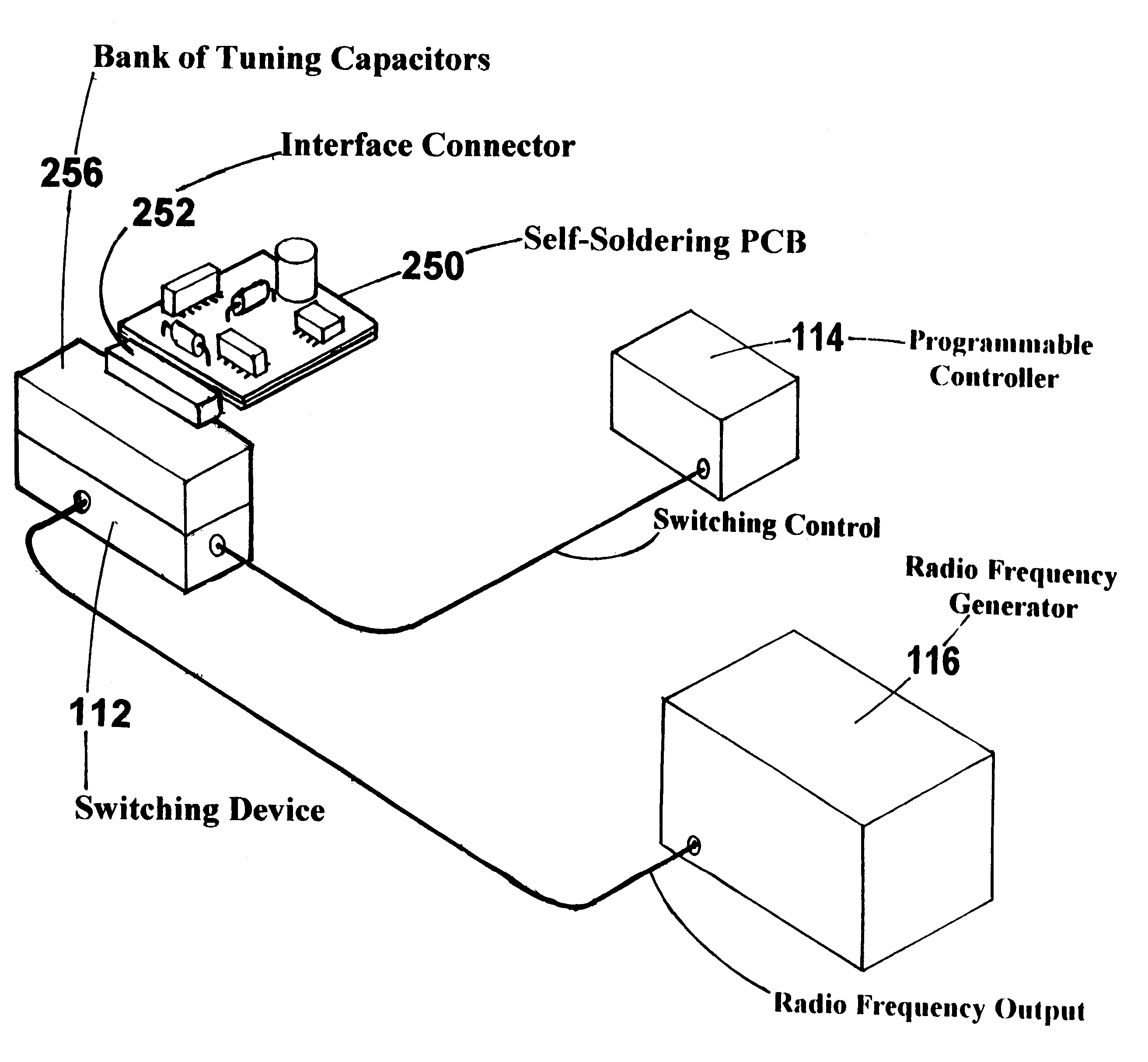
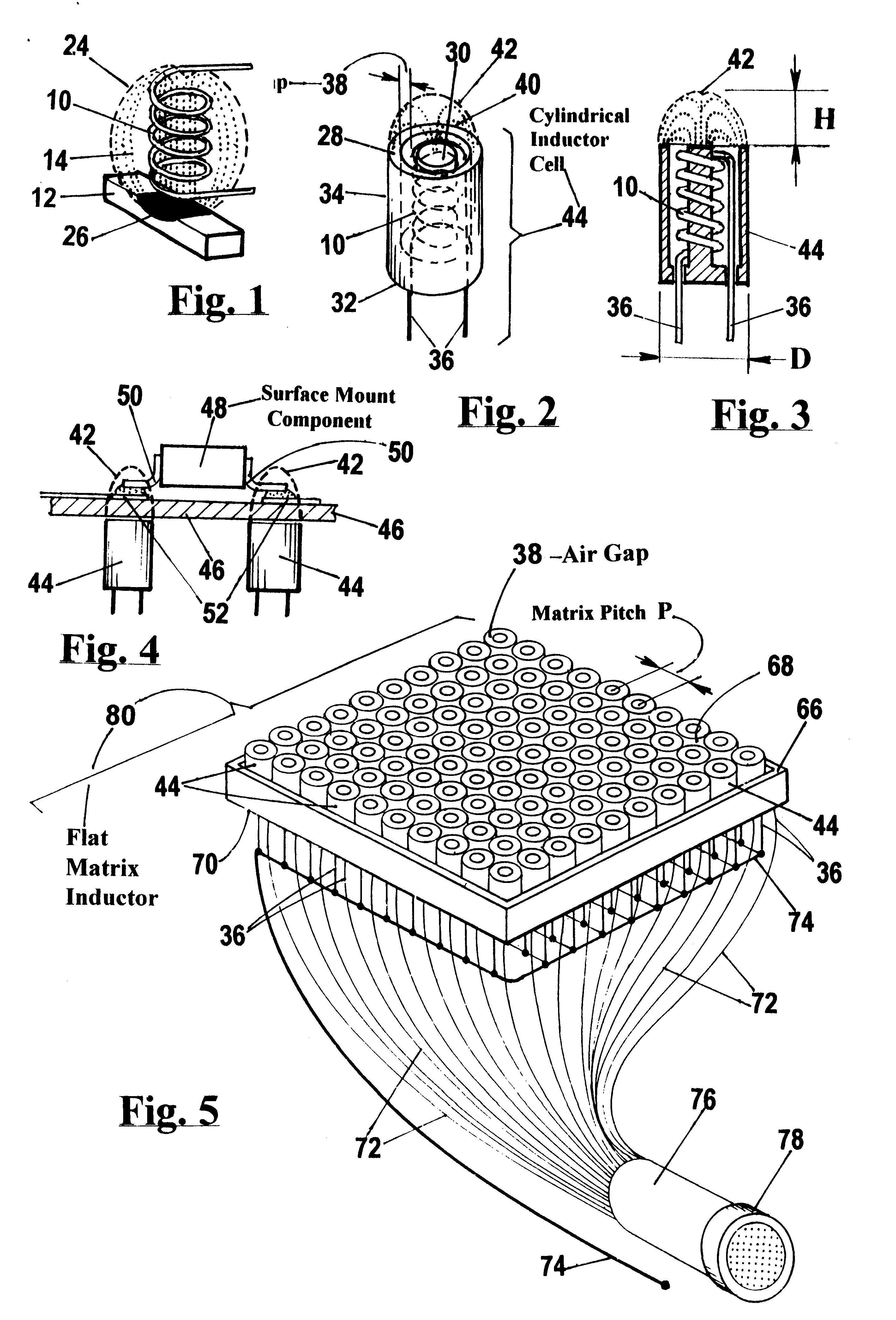
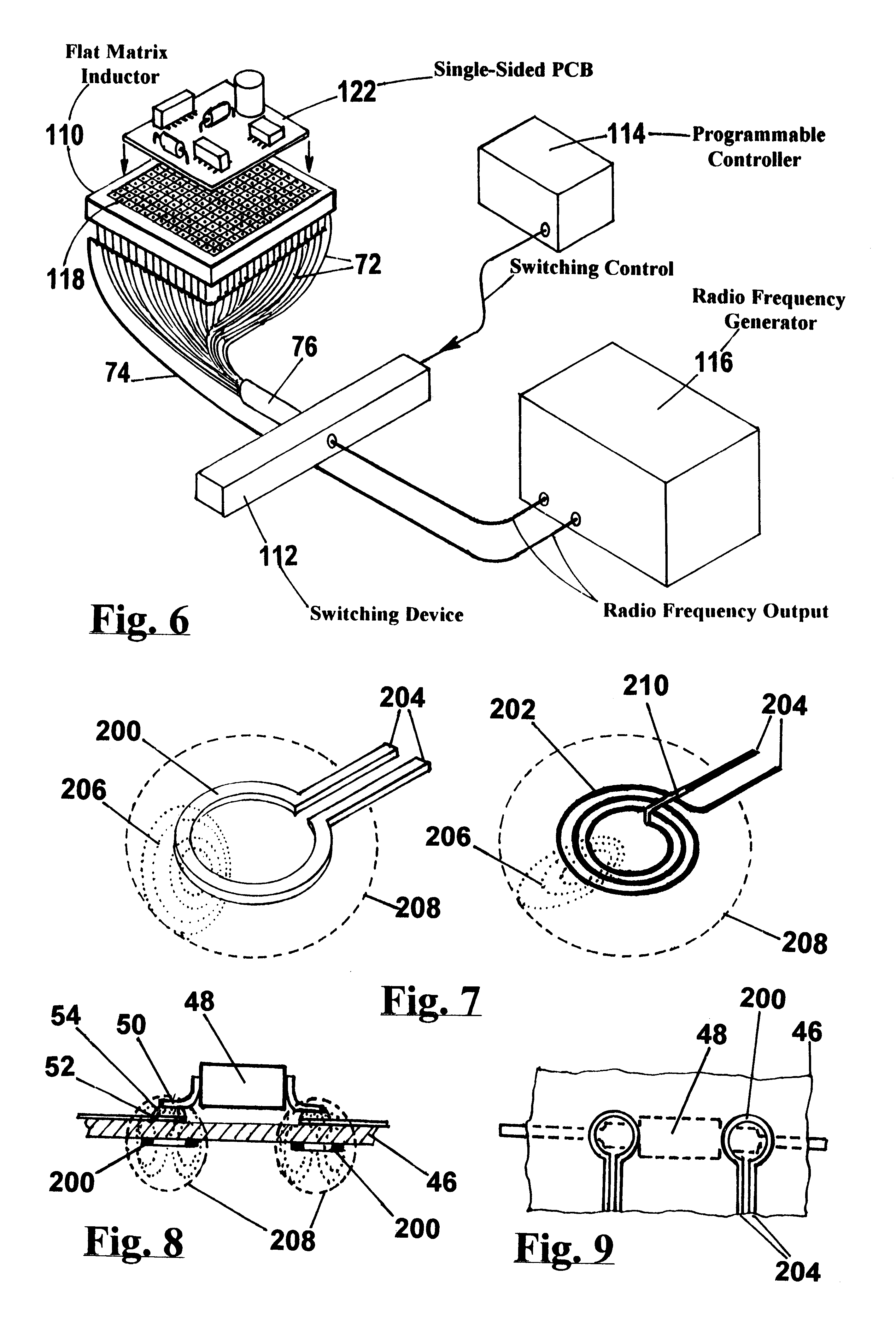
Now, aided by FIGS. 7 through 25, I shall illustrate and describe the novel and non-obvious components that form part of the embodiments of this invention. Because the actual embodiments of my invention also include items-of-commerce recognized as public-domain prior-art, the preferred embodiments will be illustrated afterwards in FIGS. 26 through 30 and described in the next part of this specification.

FIG. 7 shows, in perspective view, two basic (or simple) types of "flat" inductors that are useful for the accomplishment of this invention, (a) a flat single-turn inductor 200 and (b) a flat multi-turns inductor 202. When the two terminals 204--204 of these inductors are supplied with an alternating current each inductor generates its own variable magnetic field 206, each individual field is contained within their own variable magnetic field boundary 208 (an open-air boundary 208 is symmetric about the plane containing the flat inductor.) Notice that both terminals 204--204 of induct...


PUM

PropertyMeasurementUnit
temperatureaaaaaaaaaa
melting temperatureaaaaaaaaaa

Abstract

A new apparatus for inductively soldering surface-mount, straddle-mount and through-hole type electronic components into a self-soldering PCB (printed circuit board) in an automated fashion utilizing localized Electromagnetic Induction Heating (E.I.H.). Current manufacture technology for packaging electronic components depends on the reflow and wave soldering processes. Both processes heat up to relatively high temperatures the entire assembly, namely its PCB and all the electronic components being soldered into it. Such harsh high-temperature environment frequently causes components damage resulting in rejects and / or demanding rework. With this invention reflow oven and / or wave soldering equipment is not required. During a soldering operation only the leads and pads being soldered are heated but neither the body of said electronic components nor the dielectric material forming said self-soldering PCB and its interconnecting traces are heated. Because of this selectively localized inductive heating, the invention permits to reduce cost and improve the quality and reliability of manufactured products. The invention consumes about 200 times less energy than the reflow and wave soldering processes. This invention can readily be utilized to complement and / or supplement the reflow and wave soldering processes by providing selective inductive self-soldering of odd-form and / or heat-sensitive components. The invention also allows in-process, and in-situ, testing of soldered joints quality thus permitting rework before final assembly of a self-soldering PCB is completed. This invention also provides for a useful inductive de-soldering apparatus.

Description

This invention relates to a novel soldering apparatus for joining electronic components to a printed circuit board utilizing localized electromagnetic induction heating.BACKGROUND-DESCRIPTION OF THE PRIOR ARTThe manufacture of most modem electronic products requires a printed circuit board (PCB) that allows to electrically interconnect a variety of electronic components and also holds them together in a relatively rigid condition. Many types of components are placed over a single PCB. Electronic components such as resistors, capacitors, inductors, transformers, integrated circuit (IC) packages, connectors, headers, RF shields, LEDs, switches, board interface systems, battery sockets, etc. are electrically connected and restrained by means of soldered joints. In general, these joints are obtained by three methods: hand soldering, the wave soldering process and by the reflow soldering process.Manufacturing electronic products around PCBs requires a few sequential steps performed by di...

Claims


Application Information

Patent Timeline
Patent Type & Authority Patents(United States)
IPC IPC(8): B23K1/002H05B6/40H05K3/34H05B6/06H05B6/36H05B6/02H05B6/10
CPCB23K1/002H05B6/40H05K3/3494B23K2201/40H05B2213/03H05K3/3415H05K2203/101B23K2101/40
Inventor TRUCCO, HORACIO ANDRES
Owner TRUCCO HORACIO ANDRES
Why Eureka
Try Eureka