Integrated circuit devices and methods employing amorphous silicon carbide resistor materials

a silicon carbide resistor and integrated circuit technology, applied in the manufacture of electrode systems, electric discharge tubes/lamps, tubes with screens, etc., can solve the problems of device inoperableness, non-uniform field emission and varying brightness across the display, and limited development of high-density integrated circuit technology

Inactive Publication Date: 2001-07-31
ENTEGRIS INC +1
View PDF17 Cites 11 Cited by
  • Summary
  • Abstract
  • Description
  • Claims
  • Application Information

AI Technical Summary

Benefits of technology

It is a further object of the present invention to provide such devices and methods of fabricating the same which are inexpensive to implement.
FIG. 6 is a schematic illustration of yet still another embodiment of a field emission device in accordance with the present invention incorporating a second resistor layer for protecting a gate dielectric against electrical breakdown;

Problems solved by technology

The development of high density integrated circuit technology has been limited by the inability to provide suitable materials for integrated circuit resistor elements.
But shorts, which can occur between some of the emitters and the gate can make the device inoperable.
Variations in emitter geometries and in surface chemical properties can result in non-uniform field emission and varying brightness across the display.
Materials which require high fabrication temperatures typically are undesirable since this limits the choice of compatible materials which can withstand such high temperatures without an undesirable change in their properties.
Likewise, over time as the device is used repeatedly, the characteristics of the resistor material should either remain the same or change in a limited and predictable fashion.
While silicon has been proposed for use as such a resistor material, it is impractical to fabricate silicon resistor layers possessing sufficiently high resistivity for many applications.
To achieve high resistivity in silicon, it is necessary to deposit this material in a very pure form which substantially increases fabrication cost.
However, it has proven very difficult to provide cermet resistor layers having sufficiently high resistance, as well as to select a desired resistance of such materials through doping.
The resistivity of cermet also changes with thermal cycling and it is difficult to deposit and etch this material uniformly.
Moreover, cermet has a grain structure that leads to uneven contact with the microtip emitters of the device and consequently, affects the resistances between the emitters and cathode electrode uncontrollably.
This leads to uneven resistance values which result in non-uniform emission among the emitters.
Amorphous materials lacking such a grain structure do not share this drawback, and they are readily fabricated and processed.
However, amorphous materials are thought to be unstable, tending to change their properties substantially over time or as a result of further processing after layer formation.
Amorphous silicon with hydrogen added can have a suitably high resistivity, but hydrogen gas evolution can cause problems in amorphous materials processed at higher temperatures since it results in changes in material properties, and in some cases can form gas bubbles which disrupt the material.

Method used


Image

  • Integrated circuit devices and methods employing amorphous silicon carbide resistor materials
  • Integrated circuit devices and methods employing amorphous silicon carbide resistor materials
  • Integrated circuit devices and methods employing amorphous silicon carbide resistor materials

Examples


Embodiment Construction

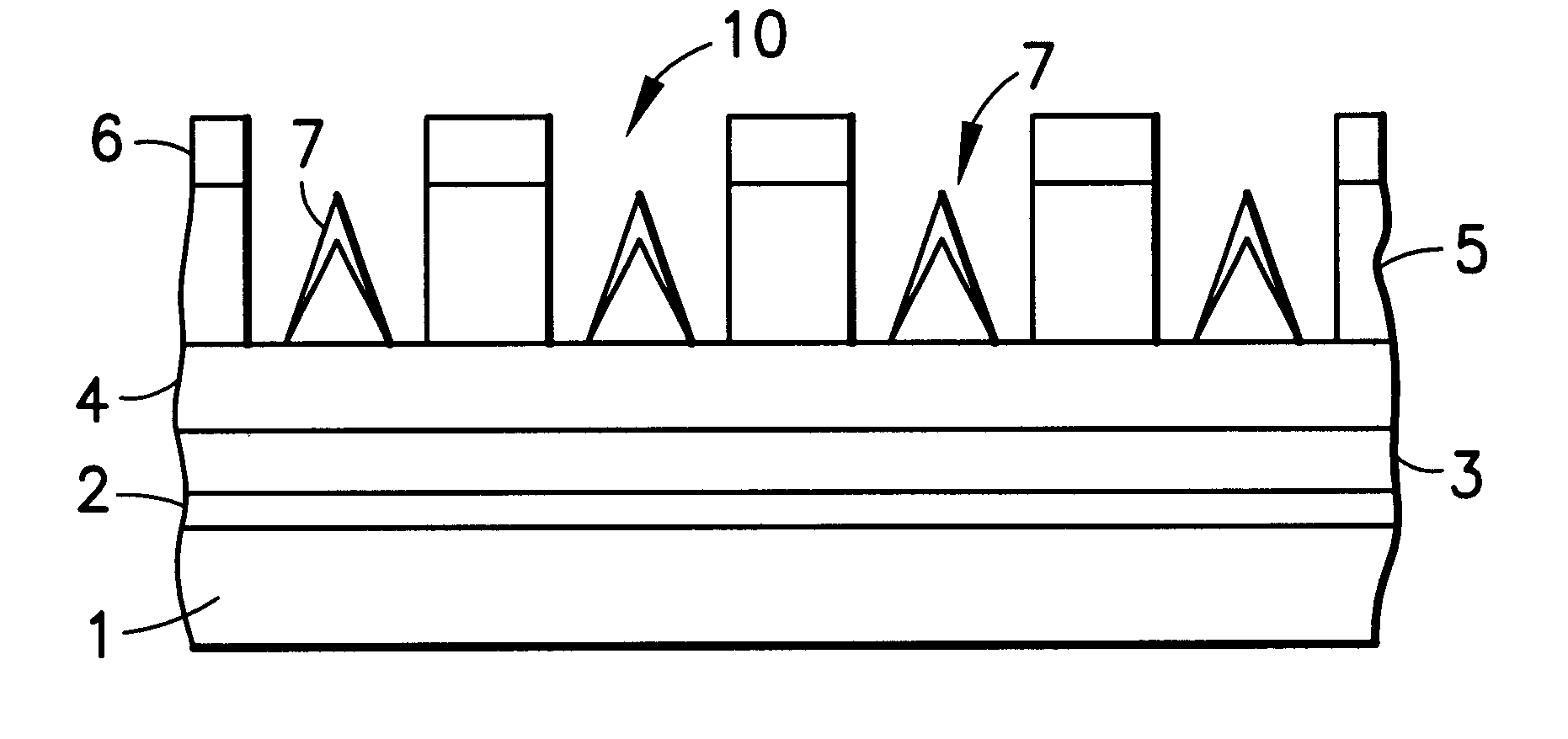
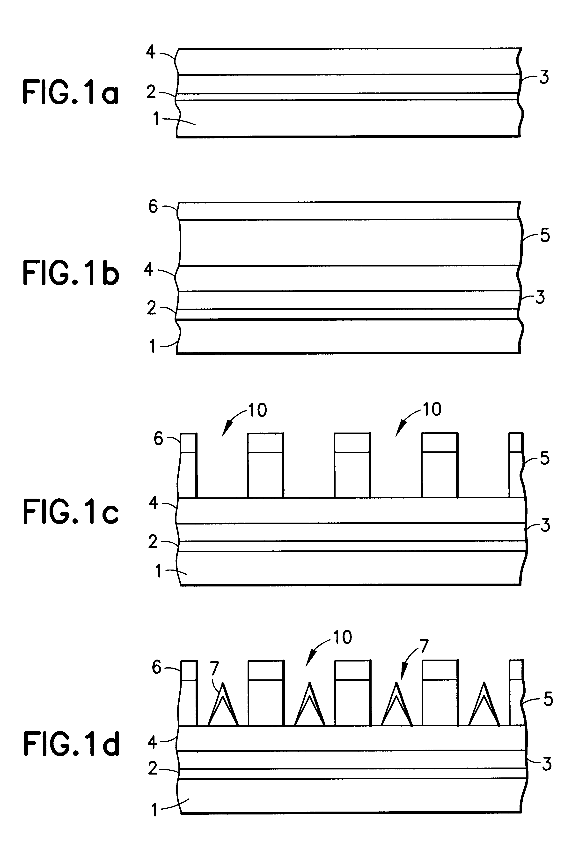
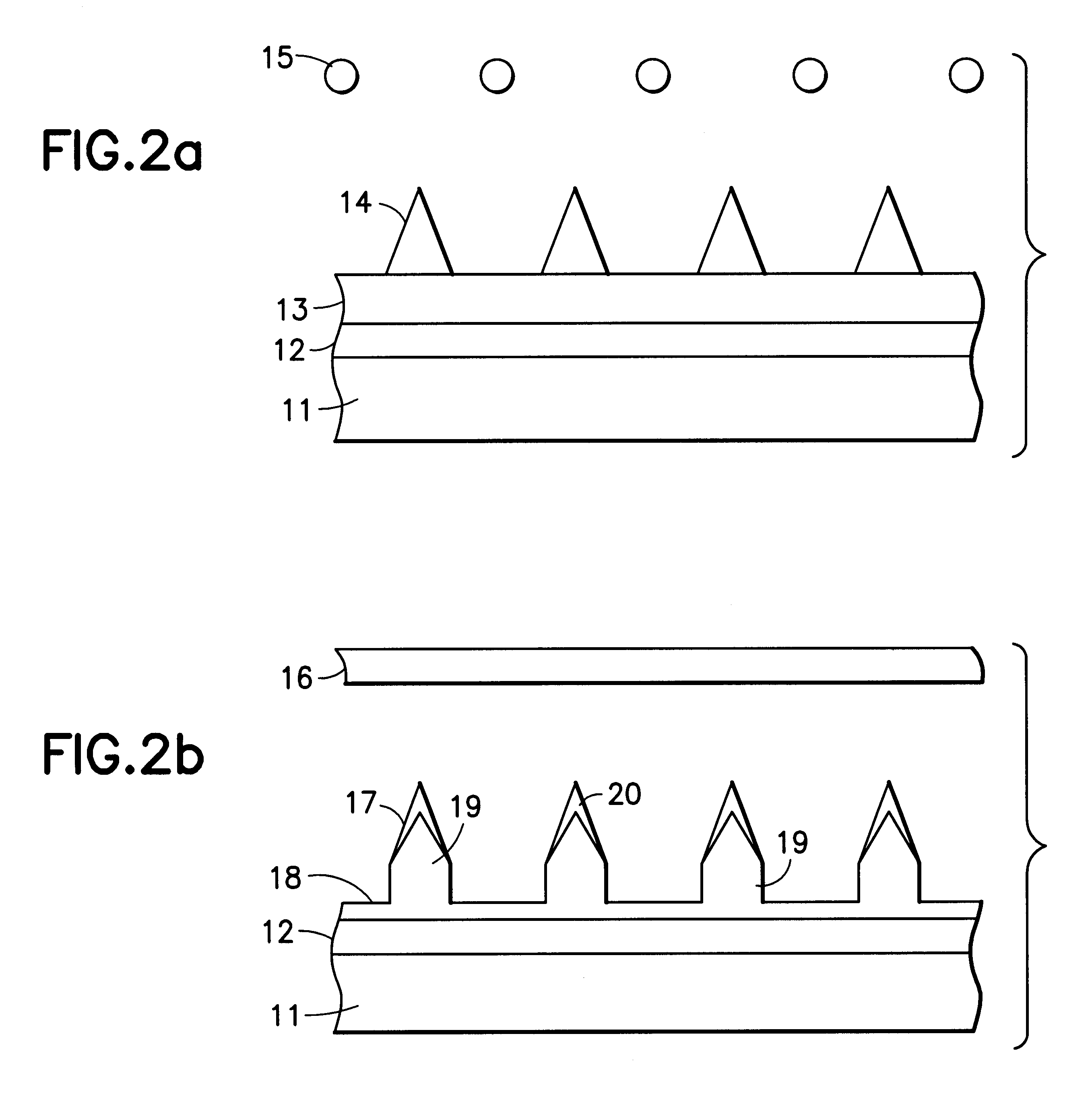
Amorphous silicon carbide resistor elements can be formed having resistivities ranging from 1 ohm cm to 10.sup.11 ohm cm. This can be accomplished by selecting the silicon to carbon ratio, by introducing impurities that act, at least in part, to terminate or eliminate dangling-bond defects, typically making the material more resistive, and / or donor or acceptor impurities at selected concentrations. In particular, nitrogen can act as a terminating species in amorphous silicon carbide, and can also form nitrides of silicon and / or carbon therein. In either case nitrogen serves to increase the resistivity of the amorphous silicon carbide, such that its resistivity increases with increasing nitrogen concentration.

The ability to select the resistivity of this material within such a large range provides substantial flexibility in selecting device geometry, affording greater circuit density. For example, for flat panel display field emission cathodes having lateral resistor geometries, rela...


PUM

PropertyMeasurementUnit
thicknessaaaaaaaaaa
thicknessaaaaaaaaaa
thicknessaaaaaaaaaa

Abstract

Integrated circuits, including field emission devices, have a resistor element of amorphous SixC1-x wherein 0<x<1, and wherein the SixC1-x incorporates at least one impurity selected from the group consisting of hydrogen, halogens, nitrogen, oxygen, sulphur, selenium, transition metals, boron, aluminum, phosphorus, gallium, arsenic, lithium, beryllium, sodium and magnesium.

Description

The present application relates to integrated circuit devices and methods which employ amorphous silicon carbide resistor materials, including field emission devices, as well as methods for fabricating and using the foregoing.The development of high density integrated circuit technology has been limited by the inability to provide suitable materials for integrated circuit resistor elements. Such materials typically must possess the ability to withstand intense electric fields without suffering breakdown, since their dimensions are so small. Moreover, the small size of these components requires high, tunable resistivity in order to achieve useful component resistances in many applications.One promising application for integrated circuit technology is in the fabrication of flat panel displays that employ cold cathode field emission. Efforts to develop such devices have sought to utilize a large number of microtip emitters in each display pixel to achieve useful field emission current ...

Claims


Application Information

Patent Timeline
Patent Type & Authority Patents(United States)
IPC IPC(8): H01L21/02H01J1/304H01J1/30H01L31/0376H01L31/036H01J9/02H01J19/24H01J21/10H01J29/04H01J31/12H01L21/822H01L27/04
CPCH01J1/3042H01L28/20H01L31/03765H01J2201/30403H01J2201/319Y02E10/548Y10S438/931H01J2329/00H01L31/0312
Inventor BRANDES, GEORGE R.BEETZ, CHARLES P.XU, XUEPINGRAMANI, SWAYAMBU V.BESSER, RONALD S.
Owner ENTEGRIS INC
Why Eureka
Try Eureka