Method for improving adhesion to copper

a technology of adhesion and copper, applied in the direction of semiconductor/solid-state device details, electrical equipment, semiconductor devices, etc., can solve the problems of reliability problems of semiconductor devices, silicon nitride does not exhibit strong adhesion to copper surfaces, and the interface between silicon nitride and copper is extremely susceptible to delamination

Inactive Publication Date: 2001-08-07
GLOBALFOUNDRIES INC
View PDF9 Cites 30 Cited by
  • Summary
  • Abstract
  • Description
  • Claims
  • Application Information

AI Technical Summary

Benefits of technology

According to the present invention, the adhesion of poorly adherent materials to a copper surface is improved by including an intervening germanium-containing layer. The germanium-containing layer can be copper germanide, germanium oxide, germanium nitride, or combinations of these layers.

Problems solved by technology

However, silicon nitride does not exhibit strong adhesion to copper surfaces.
Accordingly, the silicon nitride-to-copper interface is extremely susceptible to delamination, especially under conditions of mechanical loading.
This creates reliability problems for the semiconductor device.
Moreover, various other materials such as silicon dioxide do not adhere well to copper surfaces.
However, copper silicides exhibit a relatively high electrical resistivity and may cause an unacceptably large increase in resistance of copper interconnects.
Moreover, copper silicides have been reported to be reactive with atmospheric oxygen and tend to suffer resistivity increases upon exposure to oxygen at room temperature.
In addition, problems exist in forming the copper silicide which, in turn, leads to non-uniformity and non-repeatability of the procedure.

Method used


Image

  • Method for improving adhesion to copper
  • Method for improving adhesion to copper

Examples


Embodiment Construction

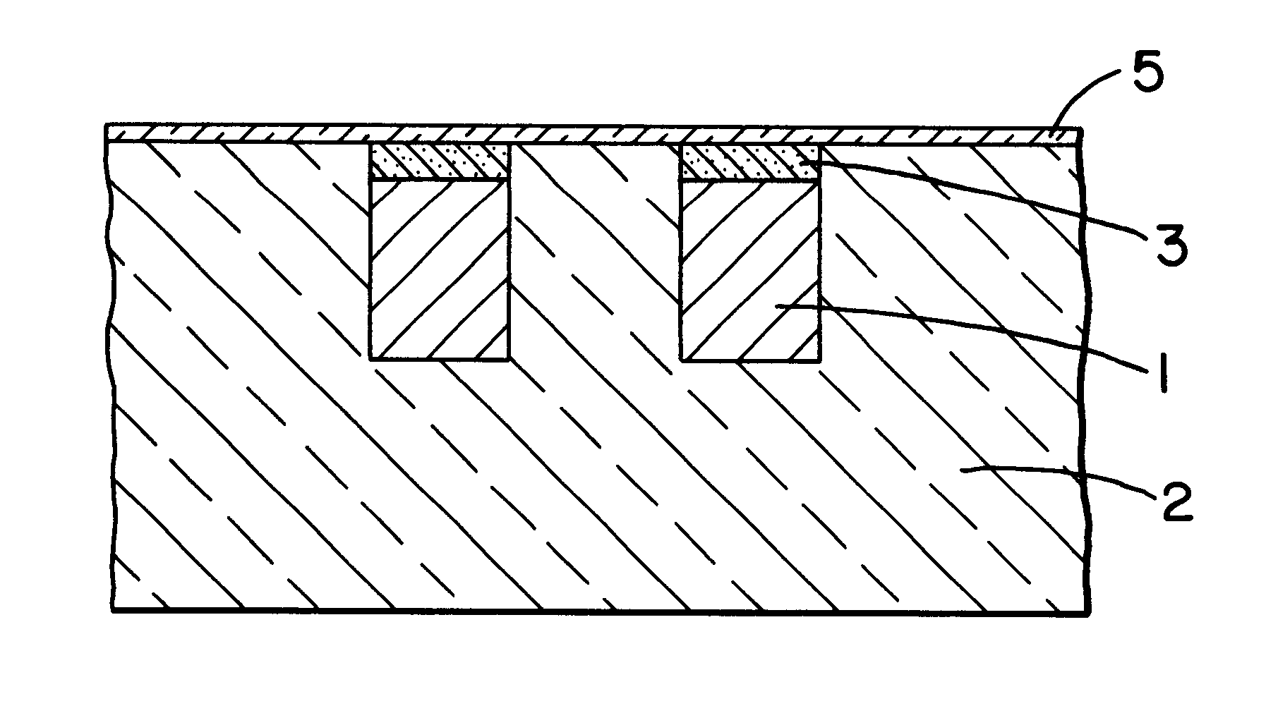
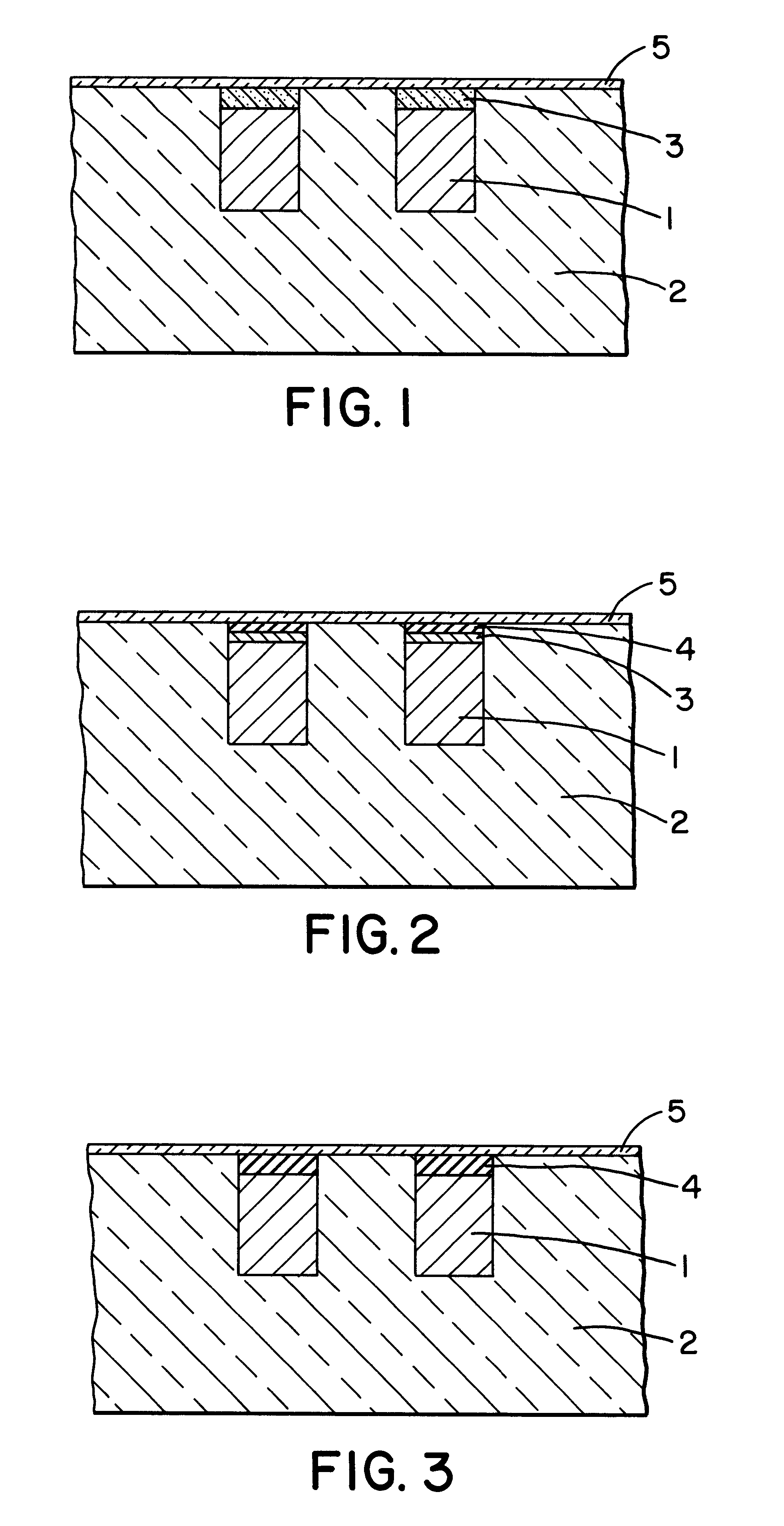
In order to facilitate an understanding of the present invention, reference will be made to the figures which are schematic diagrams of examples of semiconductor structures in accordance with the present invention.

According to the present invention, the adhesion of poorly adherent materials to a copper surface is improved by including an intervening germanium-containing layer. The germanium-containing layer can be copper germanide, germanium oxide, germanium nitride, or combinations of these layers.

As illustrated in FIG. 1, copper wiring 1 is included on a semiconductor wafer (not shown) such as silicon, silicon-germanium alloys or gallium-arsenide. The copper wiring is electrically isolated by including an interlevel dielectric 2 such as silicon dioxide (SiO.sub.2), phosphosilicate-glass (PSG), boron doped PSG (BPSG), or tetraethylorthosilicate (TEOS). In addition, the dielectric can include low dielectric constant materials such as fluorinated SiO.sub.2, organic polymers and porou...


PUM

PropertyMeasurementUnit
thicknessaaaaaaaaaa
thicknessaaaaaaaaaa
thicknessaaaaaaaaaa

Abstract

Poorly adherent layers such as silicon nitride and silicon dioxide exhibit improved adhesion to copper member by providing an intervening germanium-containing layer. The germanium-containing layer is copper germanide, germanium oxide, germanium bitride or combinations thereof. The germanium-containing layer enhances the adhesion such that the poorly adherent layer is less susceptible to delamination from the copper member.

Description

DESCRIPTION1. Technical FieldThe present invention is directed to using copper or copper alloys in semiconductor devices, and is especially directed to improving the adhesion of another layer to the copper or copper alloy.2. Background of InventionInterest in using copper as interconnects in semiconductor devices continues to increase since it possesses a lower resistivity and a reduced susceptibility to electromigration failure as compared to the more traditional aluminum or aluminum alloy interconnects.However, since copper has a tendency when used in interconnect metallurgy to diffuse into surrounding dielectric materials such as silicon dioxide, capping of the copper is essential. The capping inhibits this diffusion. One widely suggested method of capping includes employing a conductive barrier layer along the sidewalls and bottom surface of a copper interconnect. Typical of such barrier layers is tantalum or titanium. Capping of the upper surface of a copper interconnect usuall...

Claims


Application Information

Patent Timeline
Patent Type & Authority Patents(United States)
IPC IPC(8): H01L23/52H01L21/768H01L21/70H01L23/532H01L21/3205H01L21/28
CPCH01L21/76834H01L21/76849H01L21/76867H01L21/76879H01L21/76886H01L21/76888H01L23/53233H01L23/53238H01L2924/0002H01L2924/00H01L21/28
Inventor MCGAHAY, VINCENT J.IVERS, THOMAS H.LIU, JOYCE C.NYE, III, HENRY A.
Owner GLOBALFOUNDRIES INC
Why Eureka
Try Eureka