Diamond thin film or the like, method for forming and modifying the thin film, and method for processing the thin film

a technology of diamond thin film and a processing method, which is applied in the field of diamond thin film or the like, method for processing the thin film, and method for forming and modifying the thin film, which can solve the problems of not completely well understood, difficult to achieve stable and reproducible production with high efficiency, and complicated diamond formation mechanism, etc., to achieve the effect of eliminating or reducing strain, defects, color

Inactive Publication Date: 2001-09-11
APPLIED DIAMOND
View PDF18 Cites 24 Cited by
  • Summary
  • Abstract
  • Description
  • Claims
  • Application Information

AI Technical Summary

Benefits of technology

An object of the present invention is to effectively eliminate or reduce the strain, defects, color, and so on which exist in a diamond thin film or the like produced by gas phase deposition on a substrate and in a foil or plate of a free standing diamond.

Problems solved by technology

The mechanism of diamond formation is very complicated, and is not completely well understood at present.
In addition, the actual qualities of these diamonds are very sensitive to many factors, such as, gas or electron temperature, reaction gas composition, gas pressure, reaction gas flow rate, substrate material, substrate temperature, deposition machinery, and so on, and the methods do not obtain a satisfactory level of stable and reproducible production with high efficiency.
In particular, the microwave plasma CVD technique and the RF plasma CVD technique which utilize plasma discharge each have the problem of requiring complicated and expensive devices having complicated load monitoring systems for stabilizing the plasmas.
In addition, there is the disadvantage that diamond growth is very slow even when expensive devices are utilized, and high density defects or strains exist in the obtained diamond film structure.
Occasionally, the diamond thin films crack or slip off the substrates.
The occurrence of such strains is caused by defects in the diamond thin film, impurities on the grain boundary and grain boundary sections, as well as by differences in the thermal expansion characteristics between the substrate and the diamond.
In addition, even if an attempt is made to obtain a diamond thin film with specified properties, a pseudo diamond with poor characteristics is formed, a diamond-like carbon thin film is formed, or quality degradation such as the generation of graphite frequently occurs.
As described above, even if at present the CVD technique is one of the effective means for forming a diamond film, a satisfactory result is not obtained.
Thus, at present, a diamond thin film cannot be produced stably and reproducibly.
However, with respect to forming films on both sides of a substrate, there is no guarantee that the same diamond film is formed correctly and uniformly on both sides of the substrate.
Although the above reference describes a hope for uniformly forming a film so that unbalanced internal strain is eliminated, attempts have not proven satisfactory.
Moreover, it is difficult to ideally obtain such a diamond film unless the substrate heating temperature, gas flow direction for forming the film, and decomposition and deposition are precisely controlled to ensure that uniform diamonds are formed on both sides of the substrate.
This creates an additional problem that the stated device and control method must become extremely complicated and expensive.
Although all of these above stated methods provide a certain effect in reducing strain, their efficiency is small, and it is not easy to restore crystals which are damaged / roughed as suggested in the last disclosed reference.
In any case, all of the above methods do not provide an effective means for decreasing the residual strain of the diamond lattice.
These thin films consist of two- or three-components and the films readily deviate from a stoichiometric composition (in CBN, there occurs a phenomenon that the composition ratio B / N fluctuates locally), and defects or strains are more likely to occur.
However, there is still the problem that strains and defects are likely to occur during film deposition, thus making it impossible to ensure practical use.

Method used


Image

  • Diamond thin film or the like, method for forming and modifying the thin film, and method for processing the thin film
  • Diamond thin film or the like, method for forming and modifying the thin film, and method for processing the thin film

Examples


example 2

A free-standing diamond film having a thickness of greater than 100 microns and a polycrystal structure, and a free standing diamond film having a thickness of 500 microns and a polycrystal portion of preferred orientation were obtained. Irregularities which formed on the final growth face of the films were flattened, and the final growth surfaces were irradiated and heated by a microwave of 60 GHz. The modification of the films were carried out in an atmosphere containing an Argon gas flow, and the heating temperature was 800.degree. C.

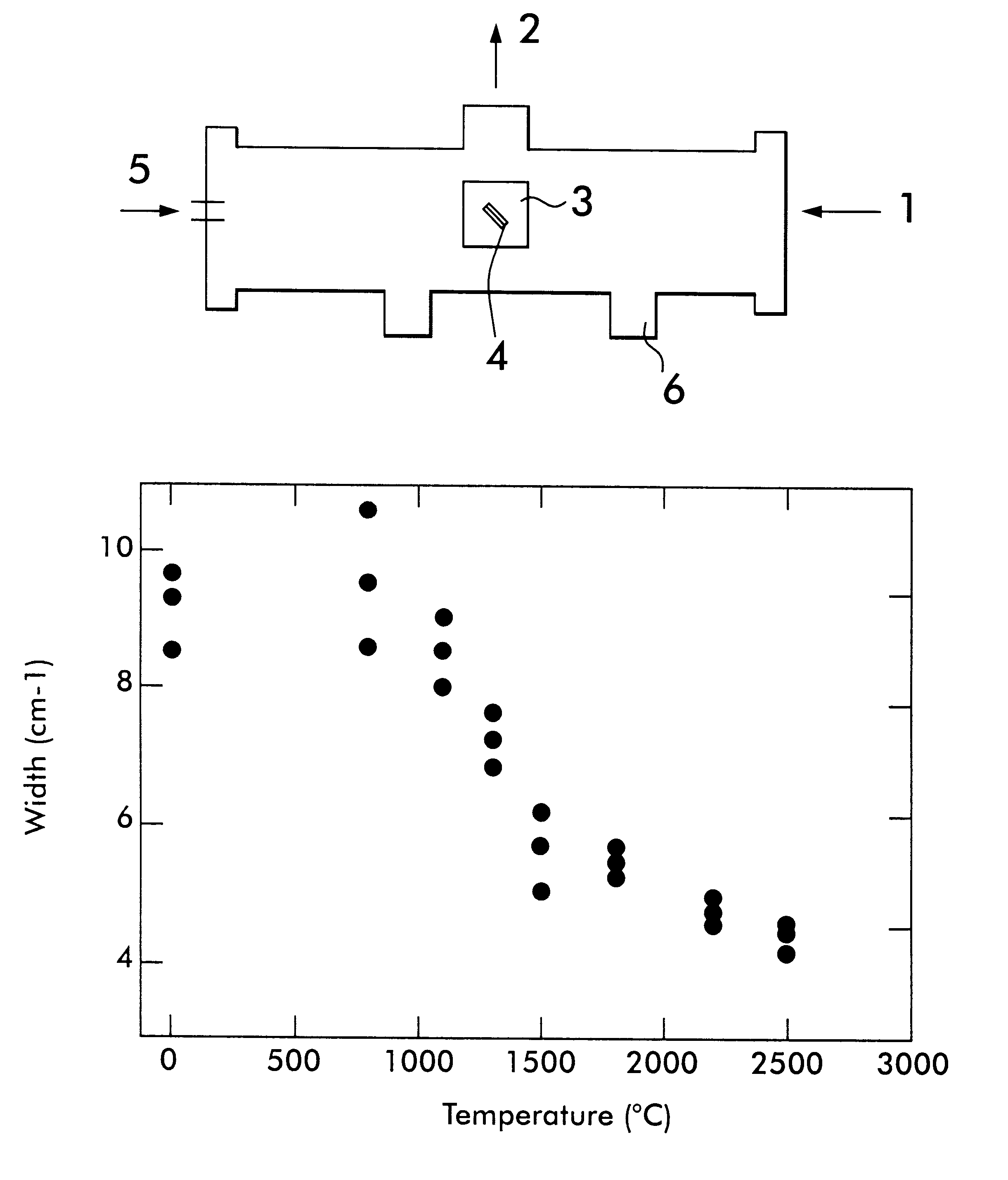
Tables 1 and 2, below, each show the relationship between the microwave outputs and the temperature (arrival temperature) being attainable with the film, ie. the same microwave power was irradiated twice against the diamond film.

The diamond thin film is heated to 800.degree. C. and is then subjected to a second separate irradiation using the same conditions. It was found that the arrival temperature is lower in the second irradiation. For instance, t...

example 3

In this example, a diamond thin film or the like was subject to microwave irradiation of 1 to 500 GHz and, at the same time, one or more gases selected from carbon, nitrogen, and boron supply source gases and gas containing semi-conductor elements were introduced. Thus, at the same time the diamond thin film or the like is being modified, a polycrystalline diamond thin film or the like, preferentially oriented polycrystalline film, single crystal thin film or a semiconductor thin film thereof is further deposited on the modified thin film element.

In a gas phase synthesizing process, as discussed above, non-diamond components are unavoidably generated in the diamond thin film. It has been found that the etching effect of atomic hydrogen generated by dissociation and activation of the carbon supply source gas (hydrocarbon / hydrogen based) generated in plasmas is effective to reduce this non-diamond component.

Therefore, in the present technique, in an attempt to qualify a polycrystallin...

example 4

A production example of a diamond based electronic device in which a part of the modified portion of the diamond thin film or the like is provided with semiconductor characteristics, is described below with respect to Example No. 4.

As in Example No. 3, a diamond thin film having a substrate is inserted into a microwave irradiation device, and a microwave was irradiated to the diamond thin film. At the same time, a carbon supply source and a gas containing Boron as a semiconductor element were introduced into the modifying atmosphere. The result was that a p-type diamond polycrystalline thin film, a preferentially oriented polycrystalline diamond thin film, and a single crystal film were further formed on the initially placed diamond thin film.

It was verified that the characteristics of the obtained semiconductor thin film provides a significant improvement due to the modification effect of microwave irradiation. In the foregoing, although an example of the diamond thin film formed o...


PUM

PropertyMeasurementUnit
thicknessaaaaaaaaaa
wavelengthaaaaaaaaaa

Abstract

An improved gas phase synthesized diamond, CBN, BCN, or CN thin film having a modified region in which strain, defects, color and the like are reduced and/or eliminated. The thin film can be formed on a substrate or be a free-standing thin film from which the substrate has been removed. The thin film can be stably and reproducibly modified to have an oriented polycrystal structure or a single crystal structure. The thin film is modified by being subjected to and heated by microwave irradiation in a controlled atmosphere. The thin film has a modified region in which a line width of the diamond spectrum evaluated by Raman spectroscopy of 0.1 microns or greater is substantially constant along a film thickness direction of the thin film, and the line width of the modified region is 85% or less of a maximum line width of the residual portion of the film thickness.

Description

The present invention generally relates to a gas phase synthesized thin film formed, for instance, by chemical-vapor-deposition (CVD) techniques. In particular, the present invention relates to a thin film made of: diamond; cubic boron nitride (CBN); boron carbon nitride (BCN), which includes a solid solution of CBN and diamond; or cubic carbon nitride (CN). (The above listed thin films will hereinafter be referred to as "diamond thin films or the like".) More particularly, the present invention relates to diamond thin films or the like in which strain, defect, color, or the like which exist in free standing foil, or plate, diamond thin films or the like are eliminated, reduced, or modified to an oriented polycrystal or single crystal structure. The present invention also relates to a method of modifying the above referenced thin films, a method of modifying and forming the above referenced thin films, and a method for processing the above referenced thin films. (Unless otherwise sp...

Claims


Application Information

Patent Timeline
Patent Type & Authority Patents(United States)
IPC IPC(8): C23C16/56C30B33/00H01L21/205H01L21/02C23C14/06C23C14/58C23C16/26C23C16/34C01B21/082C23C16/27C30B29/04
CPCC23C14/0611C23C14/0647C23C14/5826C23C16/27C23C16/34C23C16/342C23C16/56C30B33/00H01L21/0237H01L21/02527H01L21/0262C23C14/0641C30B29/04Y10T428/12542Y10T428/12535Y10S438/931Y10S118/90Y10T428/12528Y10T428/12576
Inventor MIYAKE, SHOJITAKEDA, SHU-ICHI
Owner APPLIED DIAMOND
Why Eureka
Try Eureka