

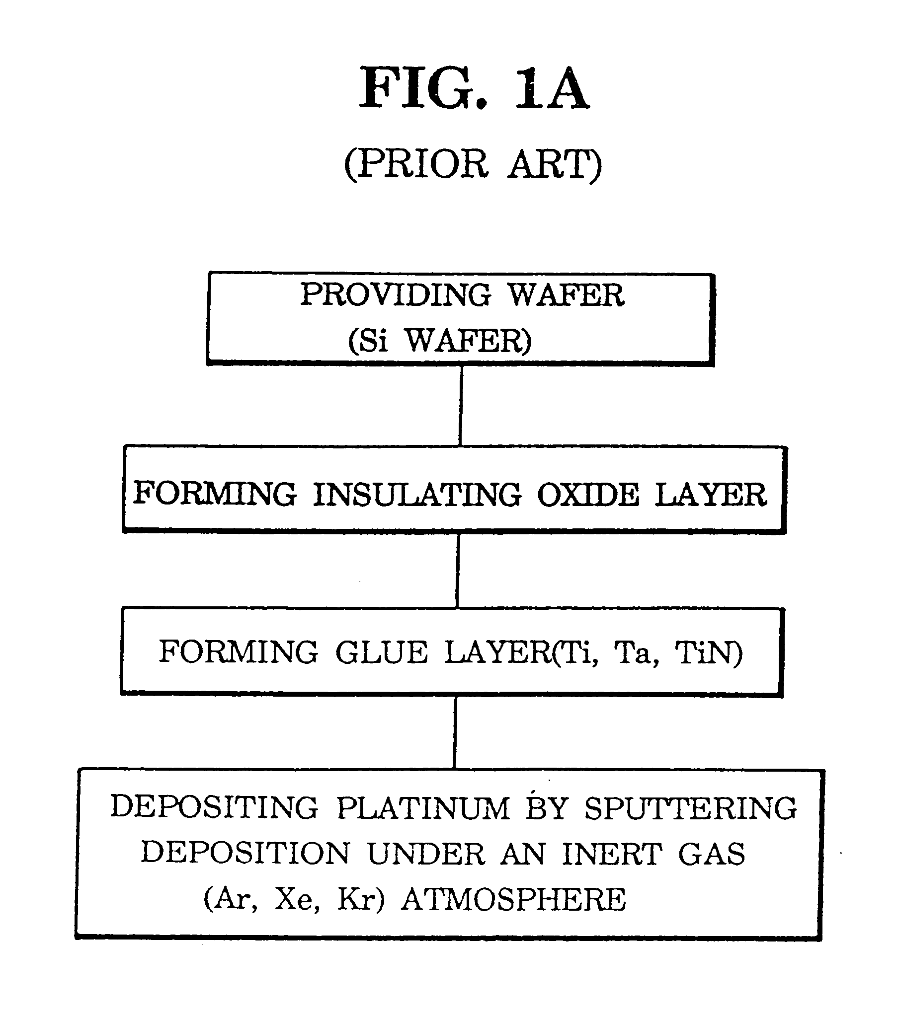
Method of forming a (200)-oriented platinum layer
a technology of platinum thin film and platinum layer, which is applied in the direction of vacuum evaporation coating, chemical vapor deposition coating, coating, etc., can solve the problems of high-dielectric oxide film formation, serious problems, and related problems
- Summary
- Abstract
- Description
- Claims
- Application Information
AI Technical Summary
Benefits of technology
Problems solved by technology
Method used
Image

Examples
example
(ii)
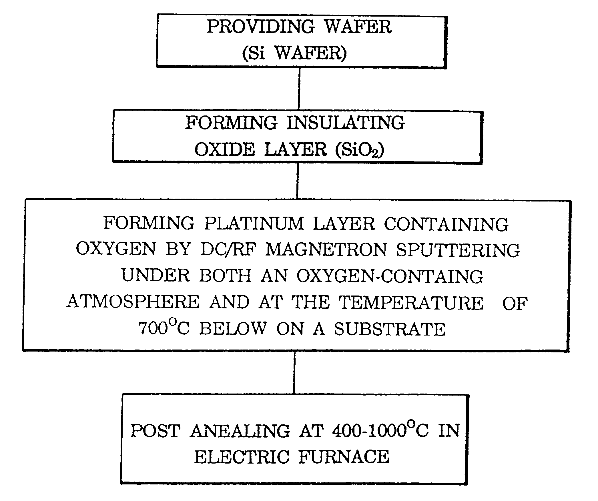
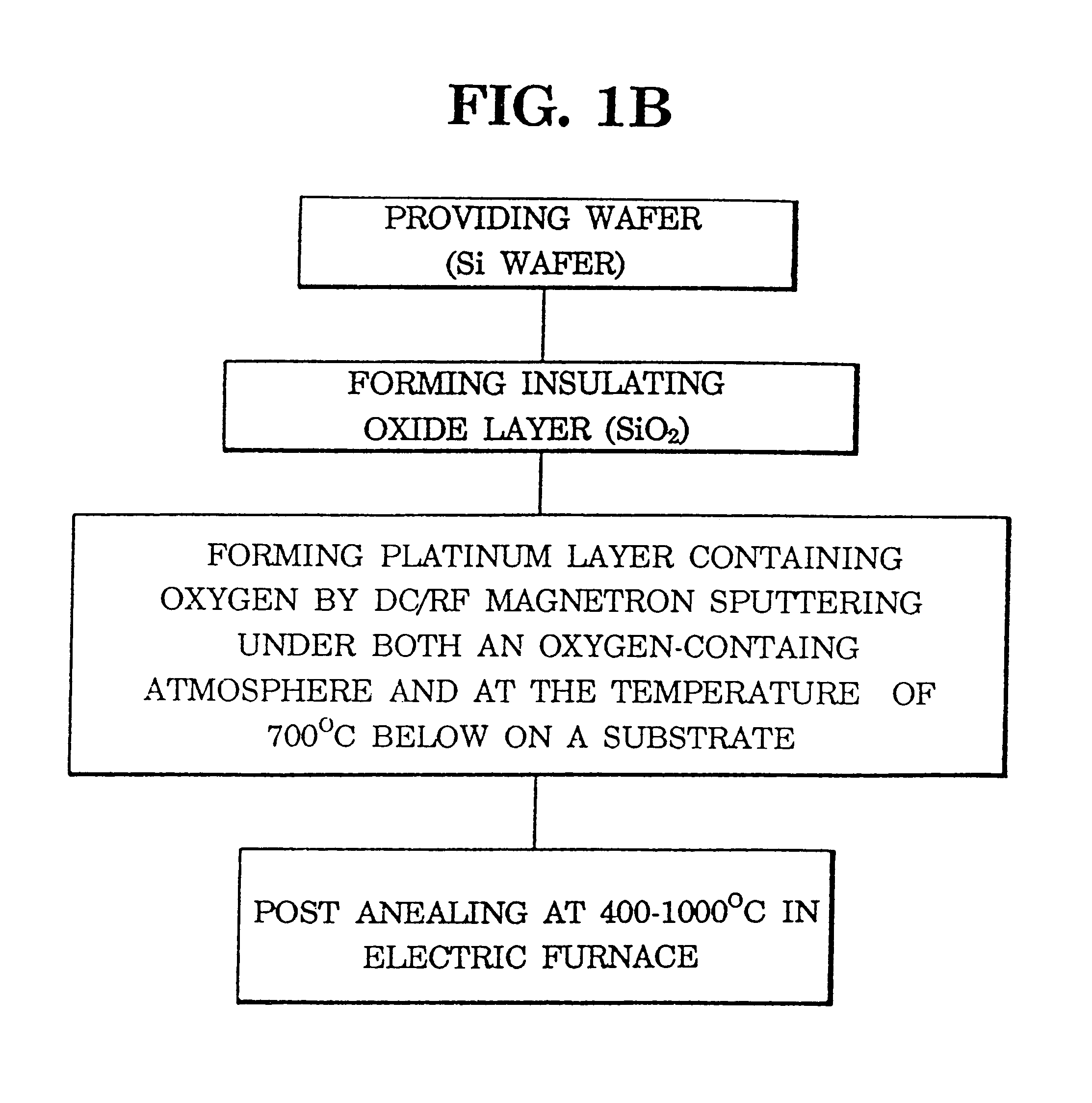
Initially, a 3,000 .ANG. SiO.sub.2 layer was formed on a 4-inch silicon wafer by the wet oxidation method.
In the next step, an oxygen containing platinum thin film was formed with an approximately 3,000 .ANG. thickness on the surface of the SiO.sub.2 layer by depositing platinum under the following conditions.
Base pressure: 2.times.10.sup.-6 Torr
Atmosphere: Ar+O.sub.2 (Ar / O.sub.2 pressure ratio: 9 / 1)
Wafer temperature: 300.degree. C.
Rotation speed of wafer; 5 rpm
Sputtering power: 130 W
Distance between target and wafer; 15 cm
In the next step, the silicon wafer was annealed in an electric furnace at a temperature between 400.degree. C. and 700.degree. C. for two and half hours.
The following table illustrates different properties such as (200) orientation degree, resistivity and formation of voids or hillocks of platinum thin films deposited on silicon wafers, according to the above example and various conventional methods of depositing a platinum thin film. In this regard, the resi...
PUM
| Property | Measurement | Unit |
|---|---|---|
| Temperature | aaaaa | aaaaa |
| Temperature | aaaaa | aaaaa |
| Temperature | aaaaa | aaaaa |
Abstract
Description
Claims
Application Information