

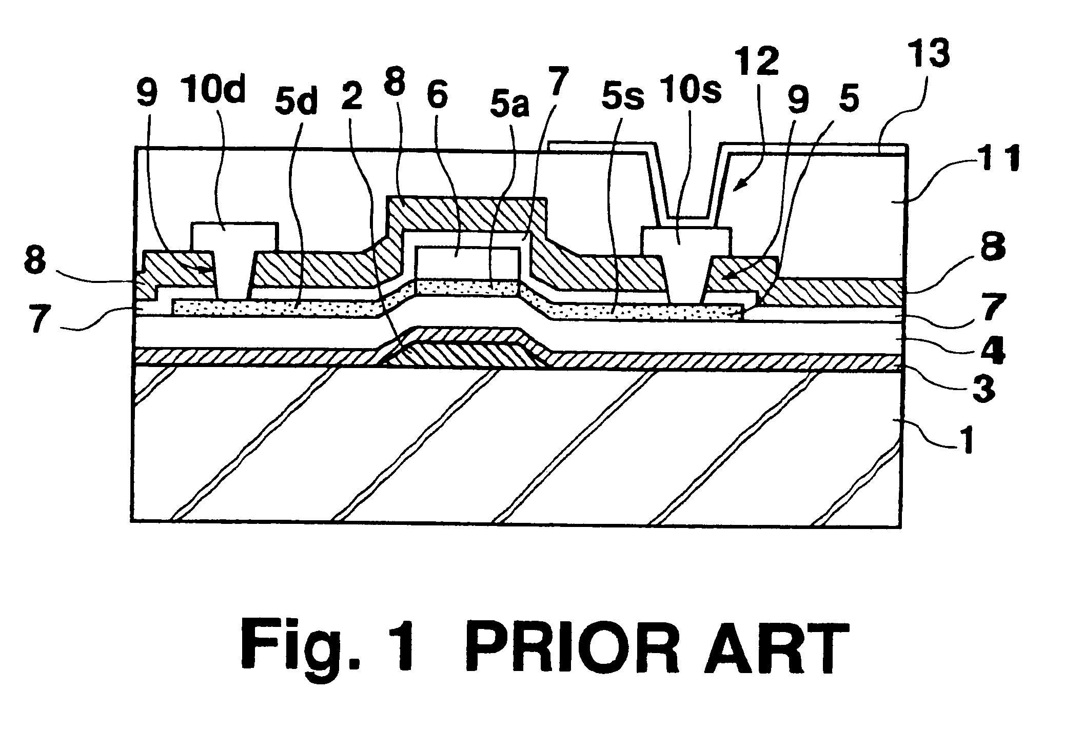
Method of manufacturing a thin film transistor
a thin film transistor and manufacturing method technology, applied in transistors, chemical vapor deposition coatings, coatings, etc., can solve the problems of deterioration of the operation characteristics of a transistor having such a polycrystalline silicon film as an active region, and the rough film surfa
- Summary
- Abstract
- Description
- Claims
- Application Information
AI Technical Summary
Benefits of technology
Problems solved by technology
Method used
Image

Examples
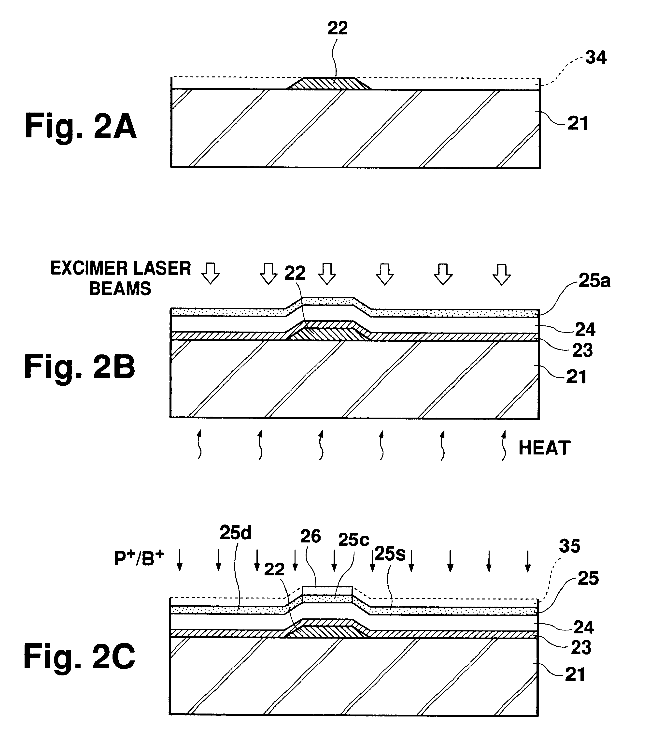
first embodiment
FIGS. 2A-2F are cross sectional views showing steps 2A-2F in a method of manufacturing a thin film transistor according to the present invention.
(a) Step 2A
On an insulating transparent substrate 21, refractory metal, such as chromium, molybdenum, aluminum, or aluminum alloy is formed by sputtering to form a refractory metal film 34. This refractory metal film 34 is patterned to a predetermined shape to form a gate electrode 22. In this patterning process, the gate electrode 22 is formed in a tapered shape by taper etching so that its width increases toward the transparent substrate 21.
(b) Step 2B
Silicon nitride is deposited on the transparent substrate 21 by plasma CVD, and subsequently silicon oxide is deposited thereon, to thereby form a silicon nitride film 23 for preventing emission of impurity ions from the transparent electrode 21 and a silicon oxide film 24 acting as a gate insulating film. Further, silicon is deposited on the silicon oxide film 23 similarly by plasma CVD to ...
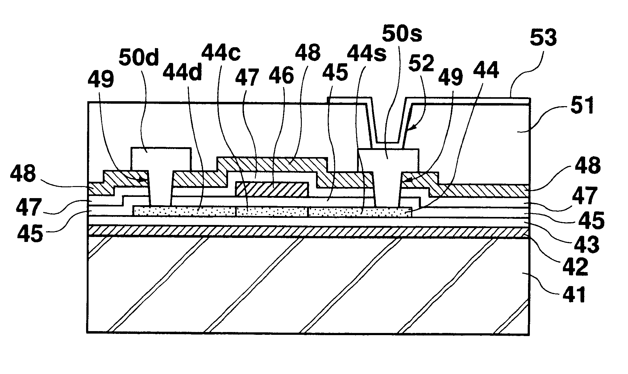
second embodiment
FIGS. 3A-3F are cross sectional views showing steps 3A-3F of the present method of manufacturing a thin film transistor.
(a) Step 3A
On an insulating transparent substrate 41, silicon nitride and then silicon oxide are deposited by plasma CVD, to thereby form a silicon nitride film 42 preventing emission of impurity ions from the transparent substrate 41, and a silicon oxide film 43 allowing deposition of a polycrystalline silicon film 44. Silicon is also deposited by plasma CVD to form an amorphous silicon film 44a. The transparent substrate 41 and the amorphous silicon film 44a are then heated to 430.degree. C. (.+-.20.degree. C.) for a period of 1 hour or longer (preferably 2 hours). This heat treatment is the same as that performed in Step 2B of the first embodiment shown in FIG. 2B. The silicon film 44a is irradiated by an excimer laser to be heated until amorphous silicon is melted. As a result, silicon is crystallized to form a polycrystalline silicon film 44.
(b) Step 3B
The pol...
PUM
| Property | Measurement | Unit |
|---|---|---|
| temperature | aaaaa | aaaaa |
| gate insulating | aaaaa | aaaaa |
| electrically conductive | aaaaa | aaaaa |
Abstract
Description
Claims
Application Information