Micromachined voltage controlled optical attenuator

a voltage control, micro-machined technology, applied in the direction of optical waveguide light guide, optical element, instrument, etc., can solve the problems of reducing the power level of an optical signal to be received, attenuating the input optical signal at the receiving end, and high price of modern optical components

Inactive Publication Date: 2002-01-29
CISCO TECH INC
View PDF12 Cites 64 Cited by
  • Summary
  • Abstract
  • Description
  • Claims
  • Application Information

AI Technical Summary

Problems solved by technology

Further, it is also often necessary to reduce the power level of an optical signal to be received by the receiving optical fiber.
The misalignment will then result in a corresponding attenuation of the input optical signal at the receiving end.
Finally, modern optical components arc often highly priced.
One of the reasons is the complicated manufacturing processes that are involved in making miniaturized, reliable components.
For example, if piezoelectric elements are used for the two prongs, while they have a short response time to the voltage applied across them, then they are subject to hysteresis, which impairs the reliability and repetitiveness of the operation of the attenuator.
Further, the electrode materials tend to migrate into the piezoelectric materials as a result of sustained voltage, causing potential short-circuiting in the piezoelectric members.
This system increases the number of electrodes that needs to be in place, thus complicating the manufacturing processes.
Further, the author suggests using a high bias voltage in the range of 100 to 300 V, together with lower control voltages in the range of 10 to 50 V. The use of a high bias voltage also decreases the practicality, flexibility and usability of this attenuation system in a fiber-optic transmission network.

Method used


Image

  • Micromachined voltage controlled optical attenuator
  • Micromachined voltage controlled optical attenuator
  • Micromachined voltage controlled optical attenuator

Examples


Embodiment Construction

The present description is of the best presently contemplated mode of carrying out the invention. This description is made for the purpose of illustrating the general principles of the invention and should not be taken in a limiting sense. The scope of the invention is best determined by reference to the appended claims.

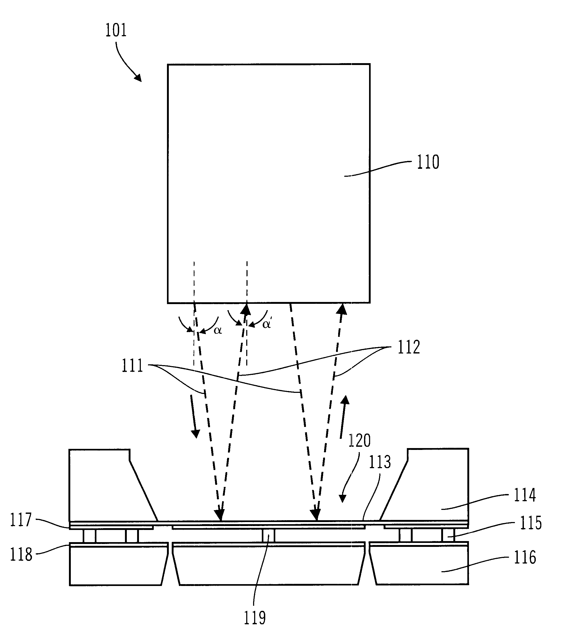
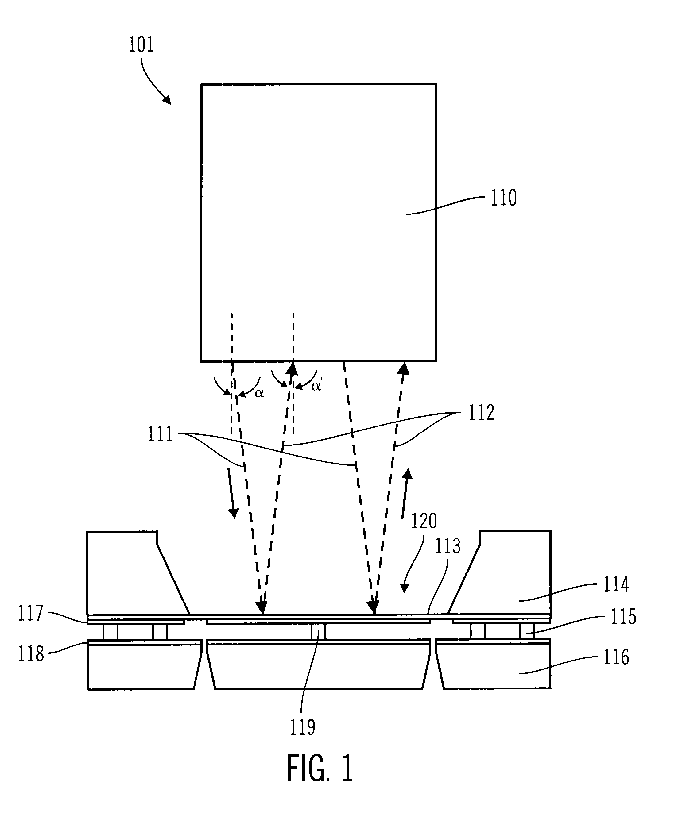
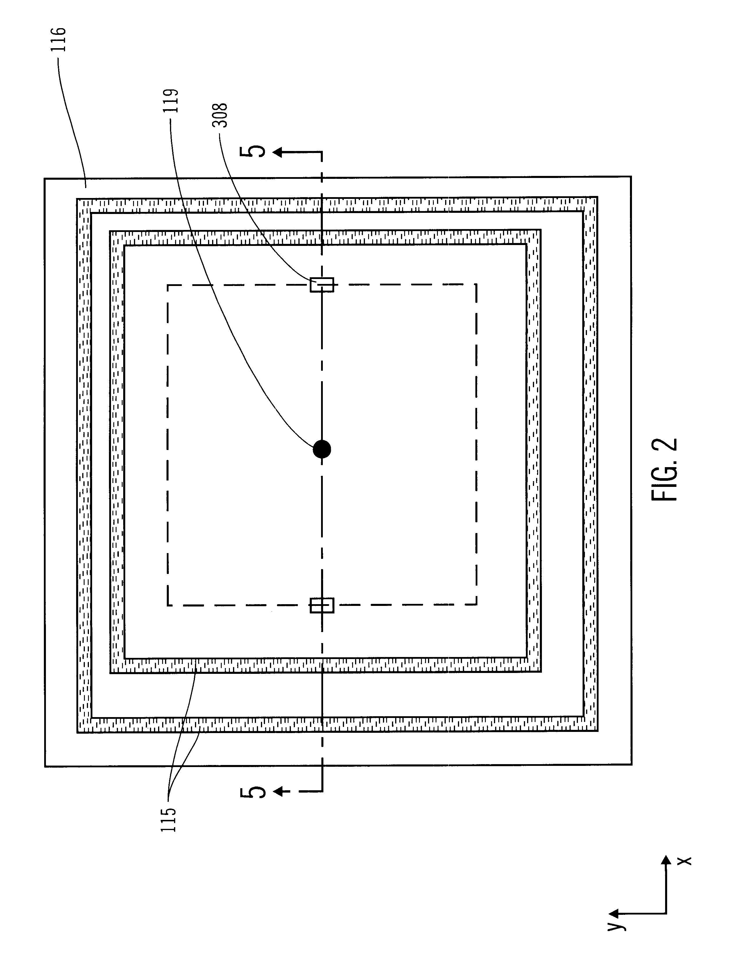
Turning first to FIG. 1, it is a schematic diagram of an optical attenuator 101 in accordance with one embodiment of the present invention. It has a planar mirror 113, which is a flexible conductive membrane, attached to an upper semiconductor structure 114. The upper semiconductor structure 114 is bonded with a lower semiconductor structure 116, separated by spacers 115. A spacing post 119 is placed between the lower and upper semiconductor structures, at or near the center of the planar mirror 113. Conductive layers 117 and 118 are coated on the bottom surface of the upper structure 114 and the top surface of the bottom structure 116. Such conductive layers can act...


PUM


Abstract

This invention provides a very sensitive optical attenuator, which can be used to couple and attenuate optical signals between optical fibers with a wide range of attenuation level. Such an optical attenuator includes a flexible conductive membrane to be moved by an external force, such as electrostatic force, to achieve deformation of the conductive membrane. The conductive membrane can be formed, for example, by a vacuum deposited silicon nitride film. A thin metallic, conductive layer is then deposited on the flexible membrane to form a reflective mirror to receive and reflect incident optical signals. The semiconductor structure includes one or more spacing posts, with which the first structural member is to be joined and bonded. Electrodes are placed on the semiconductor structure in close proximity to the flexible membrane. At various areas of the semiconductor structure, additional spacing posts are added to cause deformation of the conductive membrane when a voltage is applied between the membrane and the electrodes on the semiconductor structure.

Description

1. Field of the InventionThis invention relates to an optical attenuator, and more particularly to a voltage-controlled variable optical attenuator used in fiber-optic transmission systems, having a deformable mirror structure. This invention also relates to techniques for fabricating such an optical attenuator.2. Description of Related ArtIn a fiber-optic transmission system, it is often necessary to couple optically one or more optical fibers with one or more other optical fibers. Further, it is also often necessary to reduce the power level of an optical signal to be received by the receiving optical fiber. The device used to achieve such result is often known as an optical attenuator. For example, an optical attenuator is used to match the intensity of the incoming optical signal to the optimum operating level of a receiver. An optical attenuator is also an essential element of any gain equalization component in a fiber-optic transmission system, which aims at readjusting the po...

Claims


Application Information

Patent Timeline
Patent Type & Authority Patents(United States)
IPC IPC(8): B81B3/00G02B6/26G02B6/12G02B6/35
CPCB81B3/0051G02B6/266G02B6/3518G02B6/352B81B2201/047B81B2203/053G02B2006/12104G02B6/357G02B6/358G02B6/3584G02B6/3594
Inventor BURNS, BRENT E.HSU, TSENG-YANG
Owner CISCO TECH INC
Why Eureka
Try Eureka