Externally excited torroidal plasma source

a plasma source and torroidal technology, applied in the field of plasma reactors, can solve the problems of slow and therefore relatively less productive, difficult to process plasma of such devices, and increase the processing difficulty of such devices, so as to increase the plasma ion, increase the etch selectivity to photoresist or other materials, and increase the plasma density over the wafer

Inactive Publication Date: 2002-02-19
APPLIED MATERIALS INC
View PDF27 Cites 126 Cited by
  • Summary
  • Abstract
  • Description
  • Claims
  • Application Information

AI Technical Summary

Benefits of technology

The constriction of the torroidal plasma current path in the vicinity of the wafer or workpiece produces two independent advantages without any significant tradeoffs of other performance criteria: (1) the plasma density over the wafer is increased without requiring any increase in plasma source power, and (2) the etch selectivity to photoresist or other materials is increased, as explained above. It is believed that in prior plasma reactors it has been impractical if not impossible to increase the plasma ion density by the same step that increases etch selectivity. Thus, the dual advantages realized with the torroidal plasma source of the present invention appear to be a revolutionary departure from the prior art.

Problems solved by technology

The trend in microelectronic circuits toward ever increasing densities and smaller feature sizes continues to make plasma processing of such devices more difficult.
This task is made even more difficult because the recent trend toward shorter wavelength light for finer photolithography requires a thinner photoresist layer, so that the dielectric-to-photoresist etch selectivity must be greater than ever.
The problem with the capacitively coupled process is that it is slow and therefore relatively less productive.
Another problem that arises in such etch processes is non-uniform plasma distribution.
However, the process precursor gases tend to dissociate more rapidly in such a high density plasma, creating a higher plasma content of free fluorine, a species which reduces the etch selectivity to photoresist.
The problem is that the increase in contact opening depth and decrease in photoresist thickness to accommodate more advanced device designs has rendered the high density plasma process more likely to harm the photoresist layer during dielectric etching.
Typically, the etch stop depth is less than the required depth of the contact opening so that the device fails.
It has been difficult to realize the advantages of both types of reactors in a single machine led reactor.
One problem with high density inductively coupled plasma reactors, particularly of the type having an overhead coil antenna facing the wafer or workpiece, is that as the power applied to the coil antenna is increased to enhance the etch rate, the wafer-to-ceiling gap must be sufficiently large so that the power is absorbed in the plasma region well above the wafer.
Moreover, for high levels of RF power applied to the overhead coil antenna, the wafer-to-ceiling gap must be relatively large, and therefore the benefits of a small gap cannot be realized.

Method used


Image

  • Externally excited torroidal plasma source
  • Externally excited torroidal plasma source
  • Externally excited torroidal plasma source

Examples


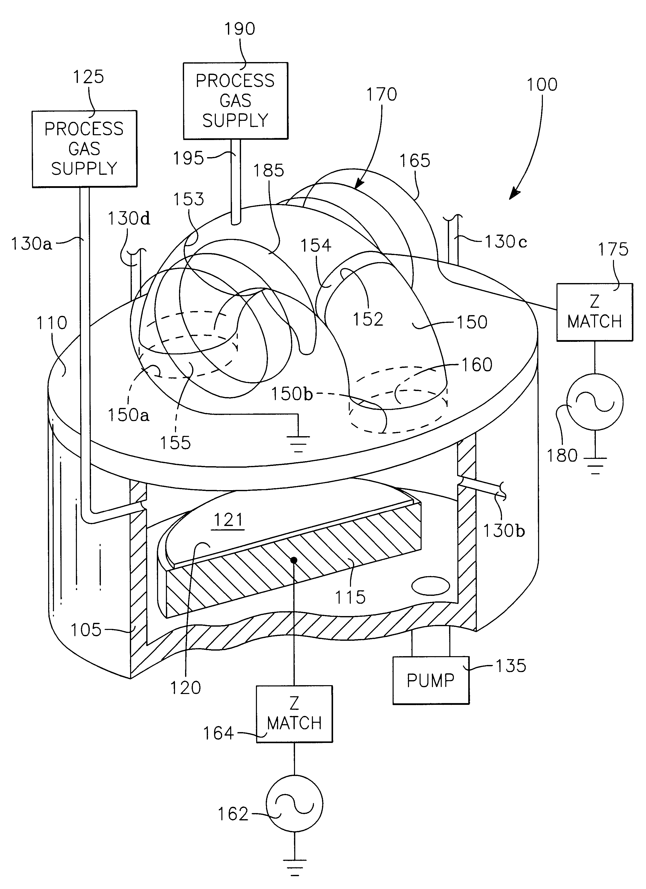
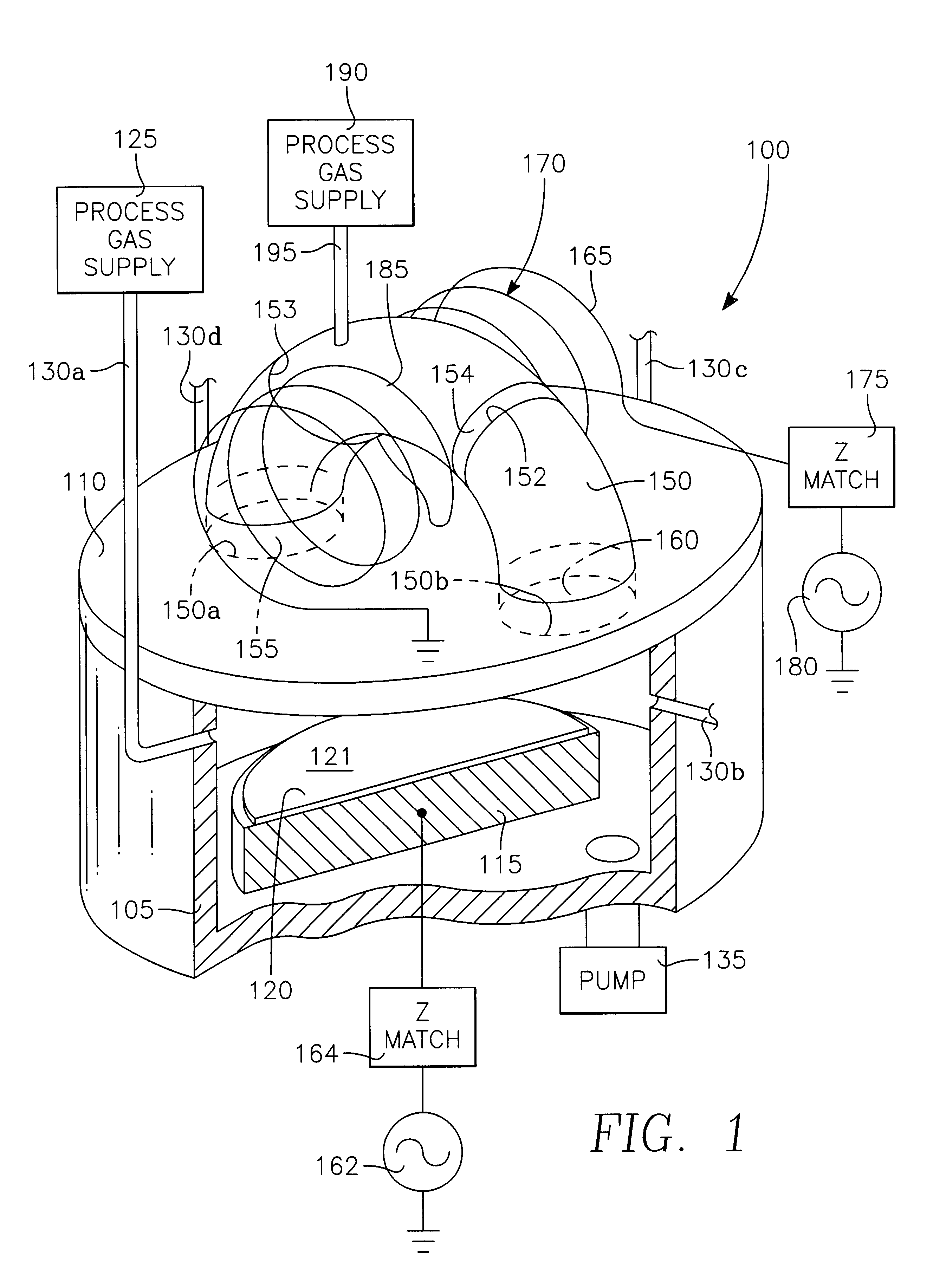
Embodiment Construction

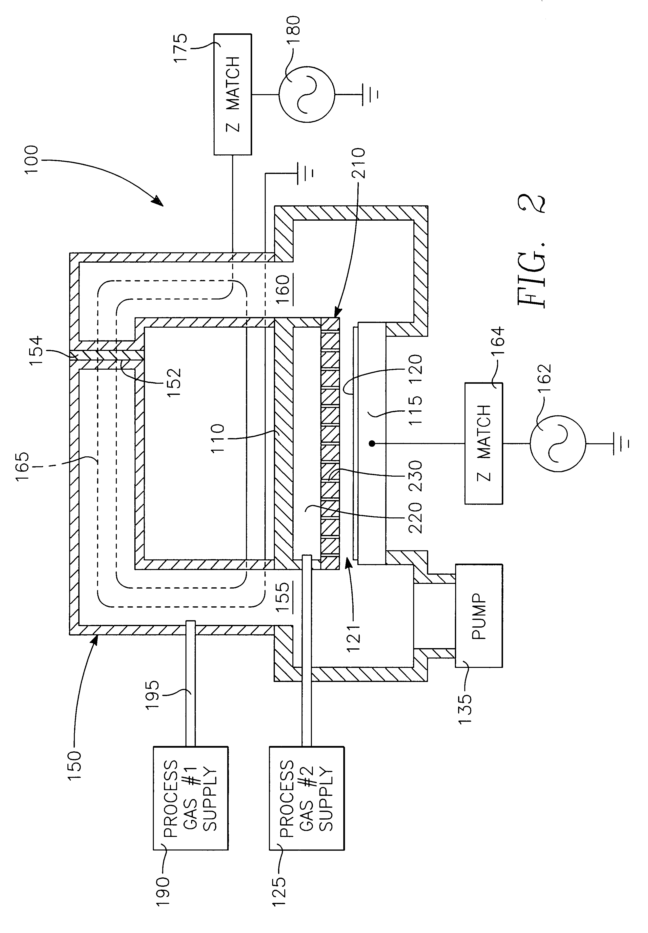
FIG. 9 illustrates a modification of the embodiment of FIG. 1 in which the side antenna 170 is replaced by a smaller antenna 910 that fits inside the empty space between the ceiling 110 and the hollow conduit 150. Preferably, the antenna 910 is a single coil winding centered with respect to the hollow conduit 150.

FIGS. 10 and 11 illustrate how the embodiment of FIG. 1 may be enhanced by the addition of a closed magnetically permeable core 1015 that extends through the space between the ceiling 110 and the hollow conduit 150. The core 1015 improves the inductive coupling from the antenna 170 to the plasma inside the hollow conduit 150.

Impedance match may be achieved without the impedance match circuit 175 by using, instead, a secondary winding 1120 around the core 1015 connected across a tuning capacitor 1130. The capacitance of the tuning capacitor 1130 is selected to resonate the secondary winding 1120 at the frequency of the RF power source 180. For a fixed tuning capacitor 1130, ...


PUM

PropertyMeasurementUnit
diameteraaaaaaaaaa
diameteraaaaaaaaaa
diameteraaaaaaaaaa

Abstract

A plasma reactor for processing a workpiece includes a chamber adapted to accept processing gases in an evacuated environment including a workpiece support, a hollow conduit defining a wall of the chamber, and having respective ends opening adjacent opposite sides of the workpiece support, and a chamber wall portion in facing relationship to the workpiece support and defining a workpiece processing zone therebetween, the processing zone and the interior of the conduit forming a torroidal interior path, and an RF energy applicator irradiating gas within the chamber to maintain a plasma within the torroidal interior path.

Description

1. Technical Field:The invention concerns plasma reactors used in processing workpieces in the manufacturing of items such as microelectronic circuits, flat panel displays and the like, and in particular plasma sources therefor.2. Background Art:The trend in microelectronic circuits toward ever increasing densities and smaller feature sizes continues to make plasma processing of such devices more difficult. For example, the diameter of contact holes has been reduced while the hole depth has increased. During plasma-enhanced etching of a dielectric film on a silicon wafer, for example, the etch selectivity of the dielectric material (e.g. silicon dioxide) to photoresist must be sufficient to allow the etch process to etch a contact hole whose diameter is ten to fifteen times its depth, without appreciably disturbing the photoresist mask defining the hole. This task is made even more difficult because the recent trend toward shorter wavelength light for finer photolithography requires...

Claims


Application Information

Patent Timeline
Patent Type & Authority Patents(United States)
IPC IPC(8): H01J37/32
CPCH01J37/321H01J37/32082
Inventor HANAWA, HIROJIYE, YANCOLLINS, KENNETH SRAMASWAMY, KARTIKNGUYEN, ANDREWTANAKA, TSUTOMU
Owner APPLIED MATERIALS INC
Why Eureka
Try Eureka