
Electronic circuit

a technology of electronic circuits and circuits, applied in the field of electronic circuits, can solve the problems of direct hazard to people, sensitivity, linearity, size, dynamic range, operating voltage, etc., and achieve the effects of improving the performance of sensors, improving the detection range, dynamic range, frequency range, and/or linearity

Inactive Publication Date: 2002-03-05
BRIDGE SEMICON
View PDF53 Cites 167 Cited by
  • Summary
  • Abstract
  • Description
  • Claims
  • Application Information

AI Technical Summary

Benefits of technology

It is an object of the present invention to provide an electronic circuit which improves the performance of sensors which produce small currents, charges, or voltages by improving their lower limits of detection, dynamic range, frequency range, and / or linearity.
By converting the signal from each pixel to a digital number during the signal collection time, blooming and saturation can be eliminated or reduced. In addition, it reduces the noise added by the circuit because an ADC that operates over a shorter time, for instance during the readout, has a greater noise bandwidth effect than the conversion strategy utilized here.

Problems solved by technology

A number of sensing media face limitations, imposed by the electronic measuring circuits, on their ability to measure physical phenomena.
The limitations imposed by the measuring circuits include sensitivity, linearity, size, dynamic range, and operating voltages.
These limitations arise from thermally-induced and / or bias currents in the components of the measuring circuit and current leakage paths over the surfaces of and / or through the components of the measuring circuit.
It presents a direct hazard to people; therefore, the measurement of radiation in various environmental settings is important.
The problem with the GM tube is that its response is not linear with the energy of the radiation so its accuracy varies with radiation photon energy, although it is useful for warning.
In this instrument, the need to amplify the radiation signal in the GM tube limits the energy linearity and thus the accuracy of the instrument.
However, at low doses and dose rates, the amount of charge generated per unit volume of gas is very small.
But, due to surface leakage currents on insulators and other circuit elements and due to other limitations within the implementing circuitry, prior art ion chambers tend to need a large volume of gas, and thus operate at high pressure or be inconveniently large, and need to employ high voltages to be sufficiently sensitive.
Most prior art capacitive sensors are limited to alternating current (AC) use because of the bias and leakage currents introduced by the prior art measurement electronics or within or over the surfaces of the capacitive sensors themselves.
Among the limitations are: (i) response time, since it takes several cycles of the AC signal for a change to be noticed, (ii) power use, because the AC signal require an AC source and constant current draw, and (iii) sensitivity, because the measurement is a small change of a large AC signal.
While this circuit is very sensitive, its usefulness is limited because of the size of the vibrating plates and the power needed to create the vibration or motion.
However, this amplification introduces some statistical noise and the electronics necessary to accomplish the high voltage multiplication are costly.
Among types of noise are shot noise, Johnson and other thermal noise sources, bias currents, leakage currents and other charge conduction paths that interfere with accurately measuring or detecting the signal.
Audio signal sensing is an especially demanding application because it requires the wide dynamic range at a relatively high frequency, up to 20 kHz.
In the case of gas detectors or electrochemical cells where there is a small signal "riding on" a significant offset, programmable gain stages will not work because no matter what the gain, the signal is of the same magnitude or significantly smaller than the offset.
CCDs have several phenomena that limit their performance, including transport noise, pixel non-uniformity, readout noise, non uniformity, non-linearity, blooming & saturation, and dark current.
Transport Noise As charge is moved from cell to cell, the efficiency of transport is not 100%.
This causes some smearing of charge from cells with more charge into cells behind them in the transport chain that have less charge.
Also, some charge may be lost to recombination as it is transported.
However, phototransistors need to operate in relatively high light levels because they do not integrate the charge or the signal.
An additional difficulty is that any blooming, saturation, smearing, or similar phenomena means that this equation no longer holds.
This also is a source of non-uniformity and non-linearity.
Also, because each pixel is being read sequentially, only a small amount of time is available for the amplifier to settle before the pixel is read.
This adds noise because the amplifier has to have a wide bandwidth to achieve the fast settling time.
But, even with these techniques to reduce or eliminate blooming, the signal still saturates.
However, larger capacitors are slower to switch, have reduced minimum light sensitivity, and thinner insulators are more likely to have pinholes, so even this reaches a limit of improvement.

Method used


Image

  • Electronic circuit
  • Electronic circuit
  • Electronic circuit

Examples


Embodiment Construction

The following description incorporates the disclosures of U.S. Pat. Nos. 4,769,547; 4,804,847 and 4,970,391 by reference, as if fully set forth herein.

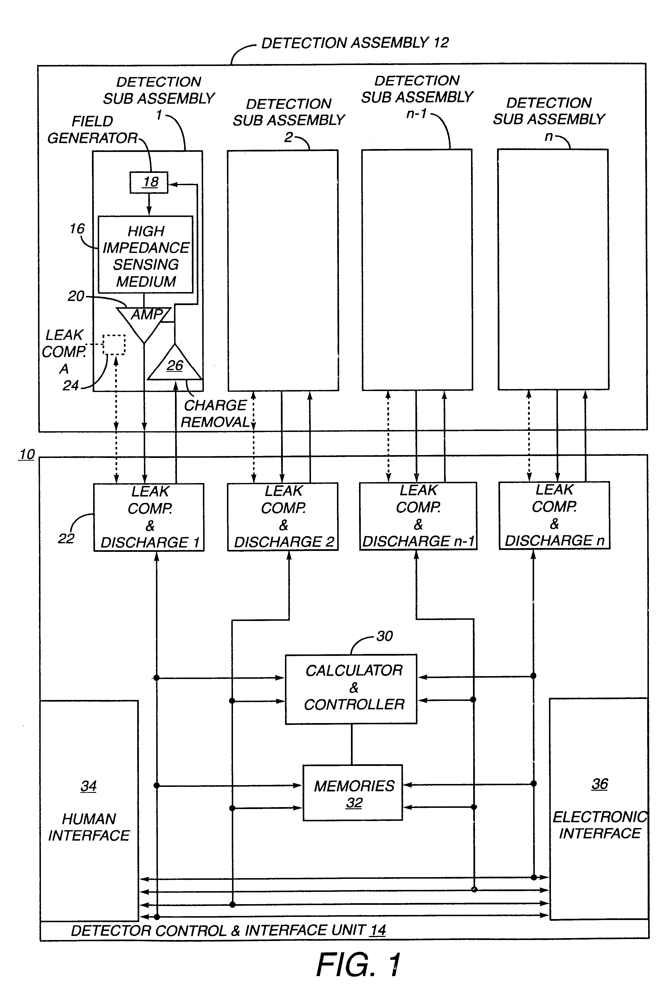
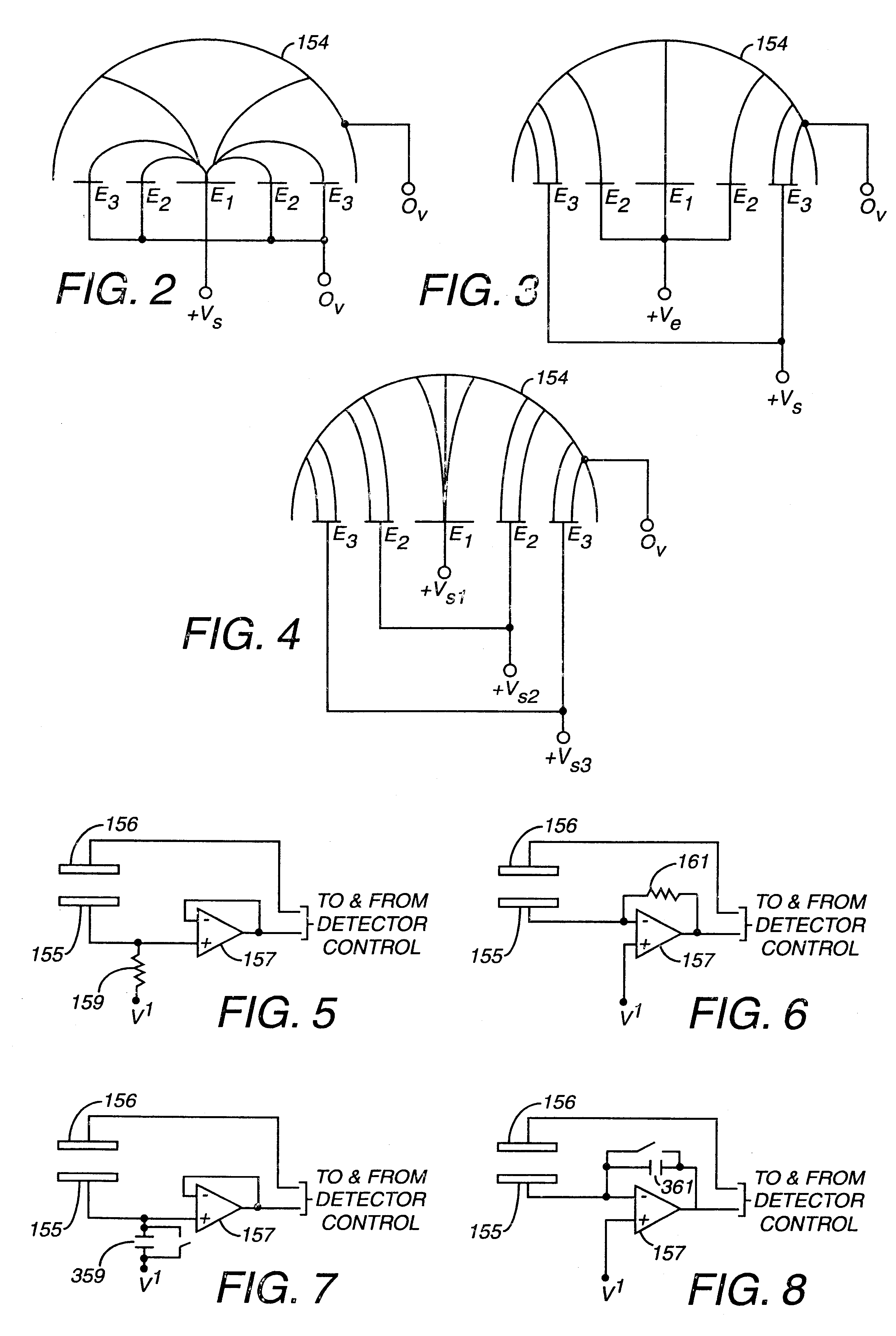
A sensing medium detects some characteristic of a physical phenomena to be measured. In the embodiment shown in FIGS. 1-10 of incorporated U.S. Pat. Nos. 4,769,547, 4,804,847 and 4,970,391, the sensing medium is configured as a radiation detector to measure the radiation level and / or dose rate of ionizing radiation incident upon an ion chamber 16 located atop an integrated circuit (IC) having a collecting or sensing electrode 155 or 170 in direct contact with the gas. In other embodiments, a variety of sensing media (including high impedance sensing media) that produce a signal by either charge or current production or induction in response to some physical phenomena occurring within the sensing media can be used with the circuitry of the present invention. These sensing media include piezoelectric, photoelectric or liquid electrochem...


PUM


Abstract

The present invention relates to an electronic circuit and an array of such circuits for precisely measuring small amounts or small changes in the amount of charge, voltage, or electrical currents. One embodiment of the present invention provides an electronic circuit for measuring current or charge that can be used with a variety of sensing media (including high impedance sensing media) that produce a signal by either charge or current production or induction in response to physical phenomena occurring within the sensing media. In another embodiment, the voltage level (bias) of either the sensing or reference electrode can be switched relative to the other upon receipt of a triggering pulse. This changes the polarity of the electric field to cause charge of the opposite polarity to be driven to the sensing electrode, thereby eliminating the need to electrically connect a discharge path to the sensing electrode to clear the charge accumulated at the sensing electrode. This can be supplemented by capacitively coupling a compensation signal to the sensing electrode to cause the amplifier output signal to lessen in magnitude below a threshold level that permits additional charge or current measurements of the same polarity before performing bias reversal. Alternately or in combination with bias reversal and capacitive compensation, sensor performance can be improved by minimizing inaccuracies caused by leakage currents or current drawn from the sensor. Other described methods of reducing leakage currents that can be used alone or in combination with the aforementioned features include the use of guard rings, physical switches or relays, the controlled creation of charges or currents of a specific polarity in a specific region of the sensing medium, controlled leakage over the surface of an insulator, and controlling the environment in which the circuit operates.

Description

The present invention relates to an electronic circuit and an array of such circuits for precisely measuring small amounts or small changes in the amount of charge, voltage, or electrical currents over a wide dynamic range.Often the measurement of a physical phenomena involves the creation of an electrical signal which is amplified and measured by an electrical circuit. A number of sensing media face limitations, imposed by the electronic measuring circuits, on their ability to measure physical phenomena. These media include solids, liquids, or gases in which the physical phenomena to be sensed causes the generation of mobile charges which then move under the influence of an electric field, or in which a charge separation is induced by the physical phenomena and / or dimensional changes in the sensing medium. Specific examples of sensing media are gases in the case of ionizing radiation, electrochemical mixtures, electret or capacitive microphones, variable capacitors, inductive picku...

Claims


Application Information

Patent Timeline
Patent Type & Authority Patents(United States)
IPC IPC(8): G01R19/25G01J1/44G01R19/00
CPCG01R19/2509G01J1/44
Inventor UBER, III, ARTHUR E.ZIFF, JOSHUA J.UBER, ROBERT E.
Owner BRIDGE SEMICON
Learn More