Ferroelectric integrated circuit having hydrogen barrier layer

a technology of integrated circuits and hydrogen barriers, which is applied in the direction of electrical equipment, semiconductor devices, capacitors, etc., can solve the problems of deterioration of the electronic characteristics of the mosfet, defects in the silicon substrate, and affecting the economical production of ferroelectric memories and other ic devices in commercial quantities

Inactive Publication Date: 2002-04-02
SYMETRIX
View PDF11 Cites 47 Cited by
  • Summary
  • Abstract
  • Description
  • Claims
  • Application Information

AI Technical Summary

Problems solved by technology

Nevertheless, the persistent problem of hydrogen degradation during the manufacturing process hinders the economical production in commercial quantities of ferroelectric memories and other IC devices using the layered superlattice material compounds with the desired electronic characteristics.
During manufacture of the circuit, the MOSFET is subjected to conditions causing defects in the silicon substrate.
As a result, numerous defects are generated in the single crystal structure of the semiconductor silicon substrate, leading to deterioration in the electronic characteristics of the MOSFET.
After the forming-gas anneal (FGA), the remnant polarization of the ferroelectrics is very low and no longer suitable for storing information.
An increase in leakage currents also results.
Thus, peeling is likely to take place at the interface between the top electrode and the ferroelectric thin film.
In addition, hydrogen also can reach the lower electrode, leading to internal stresses that cause the capacitor to peel off its substrate.
These problems are acute in ferroelectric memories containing layered superlattice material compounds because these oxide compounds are particularly complex and prone to degradation by hydrogen-reduction.
A related problem encountered in the fabrication of ferroelectric devices is the stress arising in and between the different circuit layers as a result of the manufacturing processes.
Oxygen-recovery annealing at high temperature (800.degree. C.) for about one hour results in virtually complete recovery of the ferroelectric properties degraded by hydrogen treatments; but the high-temperature oxygen-anneal itself may generate defects in silicon crystalline structure, and it may offset somewhat the positive effects of any prior forming-gas anneal on the CMOS characteristics.
Also, if hydrogen reactions have caused structural damage to the ferroelectric device, such as peeling, then a recovery anneal is not able to reverse effectively the damage.
Hydrogen degradation is also a problem in complex metal oxides used in nonferroelectric, high-dielectric constant applications in integrated circuits.
Hydrogen reactions cause structural damage, as described above for ferroelectric oxides, and cause degradation of dielectric properties.
Typically, hydrogen barrier layers known in the art are not completely effective in preventing hydrogen diffusion and the resulting hydrogen degradation of metal oxides.
Thus, even when a diffusion barrier is used, it is not uncommon for structural damage to arise in the ferroelectric or dielectric device and for hydrogen to reach the metal oxide layer and degrade the desired ferroelectric or dielectric properties of the metal oxide material.

Method used


Image

  • Ferroelectric integrated circuit having hydrogen barrier layer
  • Ferroelectric integrated circuit having hydrogen barrier layer
  • Ferroelectric integrated circuit having hydrogen barrier layer

Examples


Embodiment Construction

of the Fabrication Process

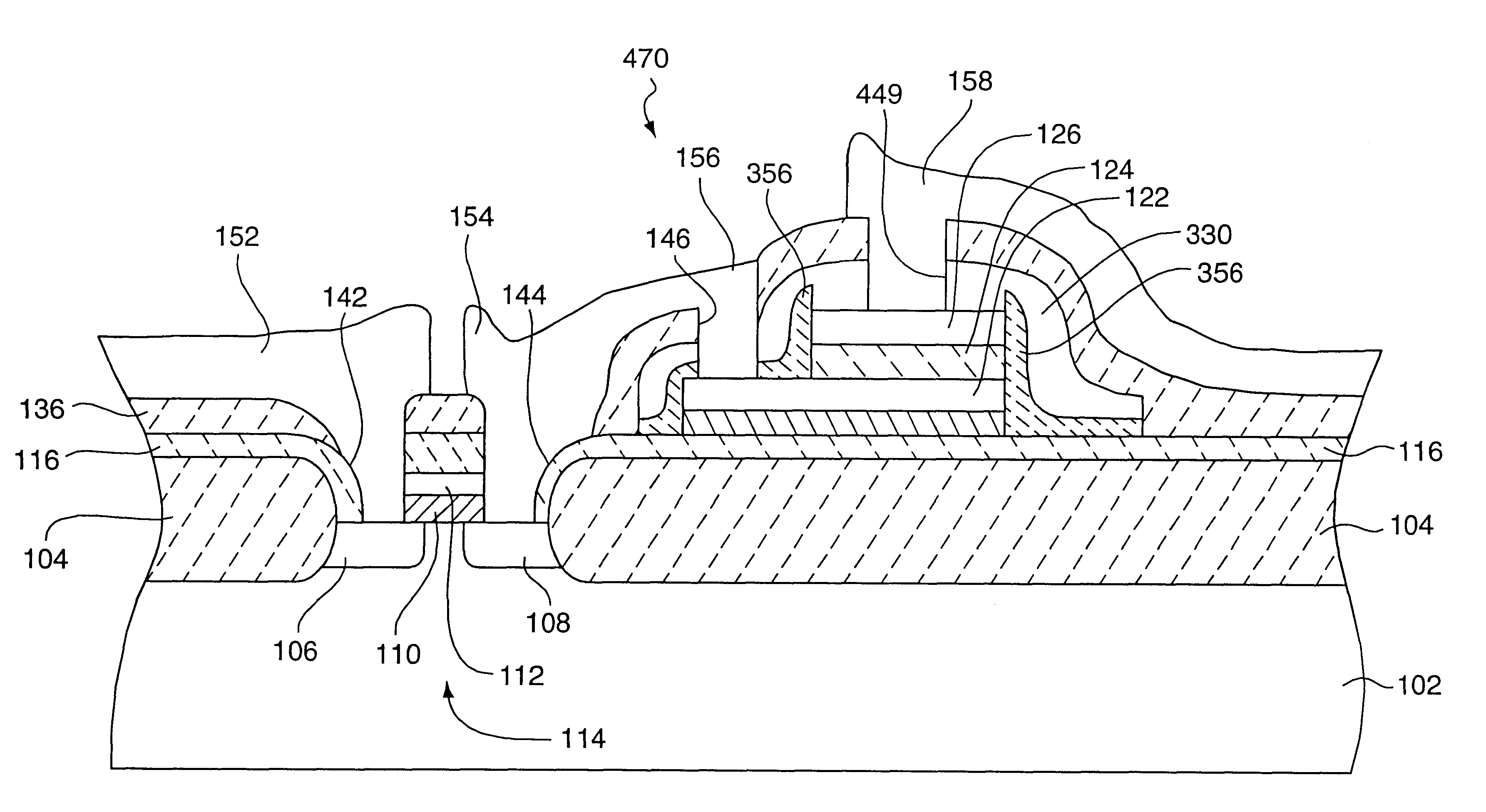
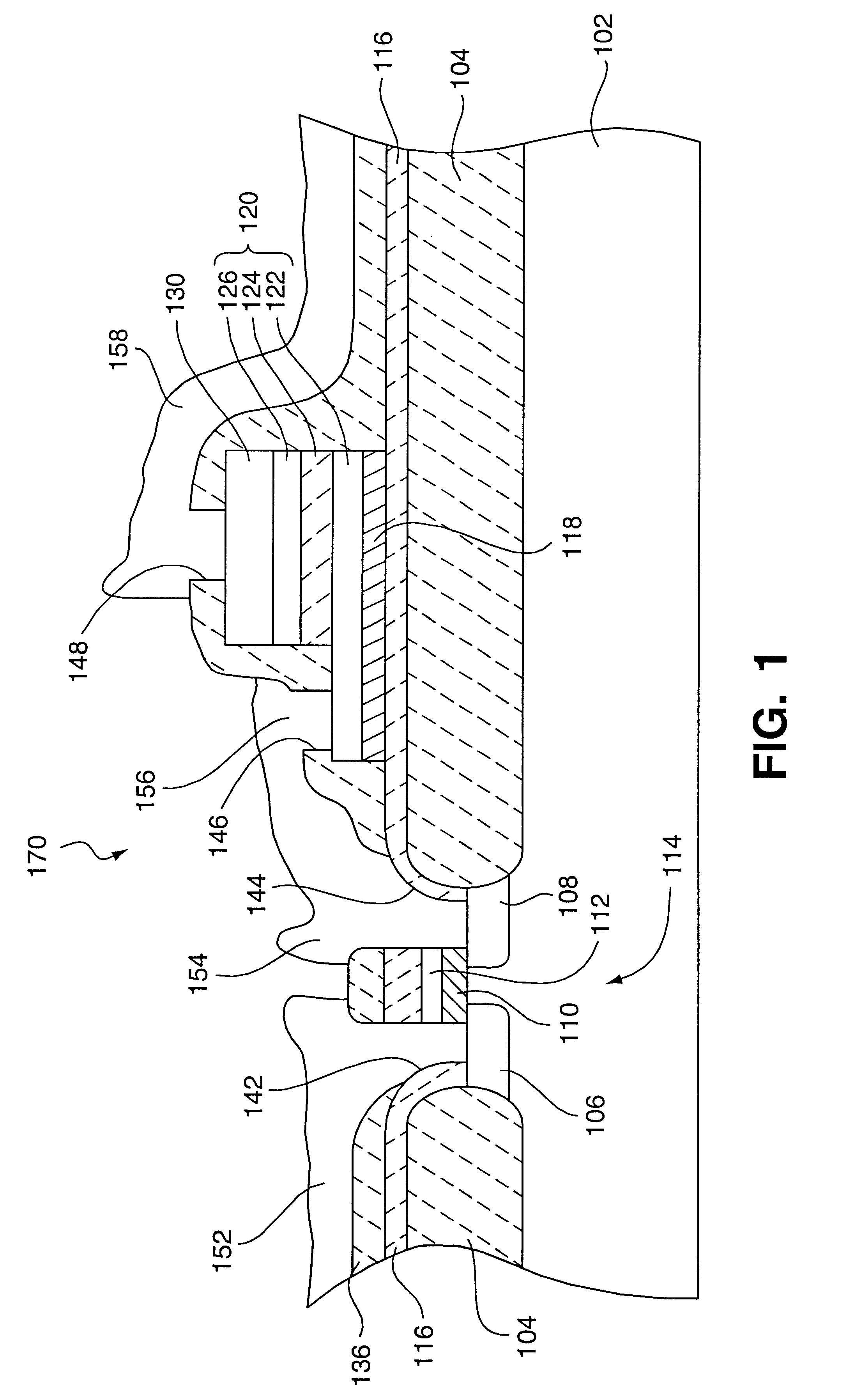
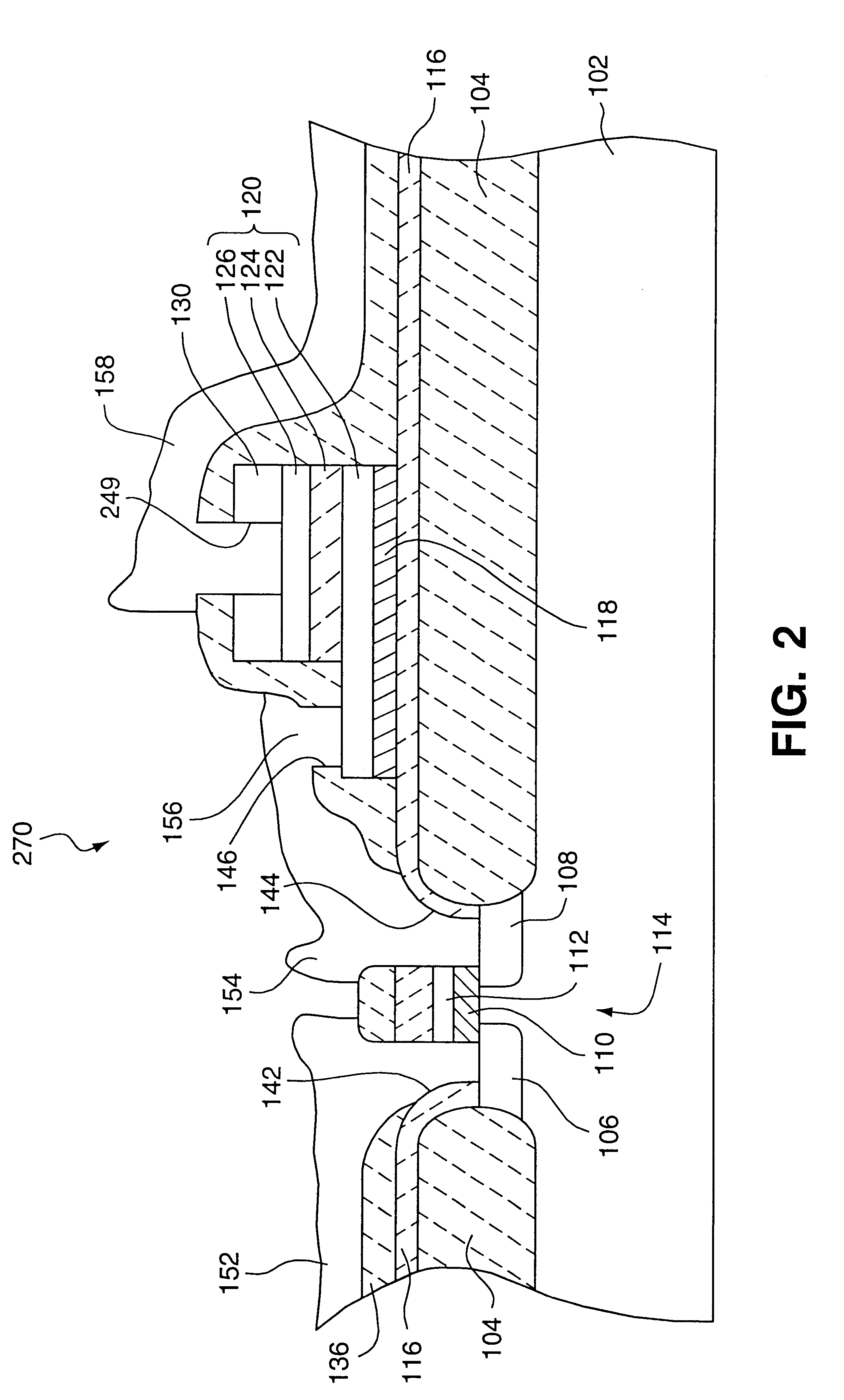
The diagram of FIG. 5 is a flow sheet of the fabrication steps to make a ferroelectric memory 170 incorporating a hydrogen barrier layer 130 in a preferred embodiment of the invention, according to FIG. 1. Ferroelectric memory 170 is preferably formed on a conventional wafer that may be silicon, gallium arsenide or other semiconductor, or an insulator, such as glass or magnesium oxide (MgO). In step 512, a semiconductor substrate 102 (FIG. 1) is provided on which a switch 114 is formed in step 514. The switch is typically a MOSFET. In step 516, a first interlayer dielectric layer 116 is formed to separate the switching element from the ferroelectric element to be formed. In step 518, a bottom electrode layer 122 is formed. Preferably, electrode layer 122 is made of platinum and is sputter-deposited to form a layer with a thickness of about 200 nm. In the preferred method, an adhesion layer 118 made of titanium or titanium nitride of about 20 nm would be for...


PUM

PropertyMeasurementUnit
temperatureaaaaaaaaaa
thicknessaaaaaaaaaa
thicknessaaaaaaaaaa

Abstract

A hydrogen diffusion barrier in an integrated circuit is located to inhibit diffusion of hydrogen to a thin film of metal oxide material in an integrated circuit. The hydrogen diffusion barrier comprises at least one of the following nitrides: aluminum titanium nitride (Al2Ti3N6), aluminum silicon nitride (Al2Si3N6), aluminum niobium nitride (AlNb3N6), aluminum tantalum nitride (AlTa3N6), aluminum copper nitride (Al2Cu3N4), tungsten nitride (WN), and copper nitride (Cu3N2). The thin film of metal oxide is ferroelectric or high-dielectric, nonferroelectric material. Preferably, the metal oxide comprises ferroelectric layered superlattice material. Preferably, the hydrogen barrier layer is located directly over the thin film of metal oxide.

Description

1. Field of the InventionThe invention relates to an integrated circuit having a hydrogen barrier layer to protect elements containing ferroelectric or high-dielectric constant metal oxide materials.2. Description of the Related ArtFerroelectric compounds possess favorable characteristics for use in nonvolatile integrated circuit memories. See Miller, U.S. Pat. No. 5,046,043. A ferroelectric device, such as a capacitor, is useful as a nonvolatile memory when it possess desired electronic characteristics, such as high residual polarization, good coercive field, high fatigue resistance, and low leakage current. Lead-containing ABO.sub.3 -type ferroelectric oxides such as PZT (lead titanate zirconate) and PLZT (lanthanum lead titanate zirconate) have been studied for practical use in integrated circuits. Layered superlattice material oxides have also been studied for use in integrated circuits. See Watanabe, U.S. Pat. No. 5,434,102. Layered superlattice material compounds exhibit chara...

Claims


Application Information

Patent Timeline
Patent Type & Authority Patents(United States)
IPC IPC(8): H01L21/02H01L27/115
CPCH01L27/11502H01L28/55H01L28/75H01L2924/0002H01L2924/00H10B53/00
Inventor CUCHIARO, JOSEPH D.PAZ DE ARAUJO, CARLOS A.MCMILLAN, LARRY D.
Owner SYMETRIX
Why Eureka
Try Eureka