Method for cleaning semiconductor wafer after chemical mechanical polishing on copper wiring

a technology for cleaning semiconductor wafers and copper wiring, which is applied in the direction of cleaning using liquids, semiconductor/solid-state device details, and lapping machines, etc., can solve the problems of contaminant deterioration of circuit components, present inventors cannot find any surface cleaning, and diluted hydrofluoric acid is not suitable for surface cleaning

Inactive Publication Date: 2002-05-14
RENESAS ELECTRONICS CORP
View PDF14 Cites 46 Cited by
  • Summary
  • Abstract
  • Description
  • Claims
  • Application Information

AI Technical Summary

Problems solved by technology

The contaminant deteriorates the circuit components.
However, the present inventors could not find any surface cleaning.
For this reason, the diluted hydrofluoric acid is not appropriate for the surface cleaning after the chemical mechanical polishing on the tungsten wiring laminated on the barrier metal layer.
The diluted hydrofluoric acid etches the barrier metal layer at a large etching rate, and was not available for the post cleaning.
Although the aqueous ammonia removed the particles from the copper wiring, a large number of pits were produced in the

Method used


Image

  • Method for cleaning semiconductor wafer after chemical mechanical polishing on copper wiring
  • Method for cleaning semiconductor wafer after chemical mechanical polishing on copper wiring
  • Method for cleaning semiconductor wafer after chemical mechanical polishing on copper wiring

Examples


first example

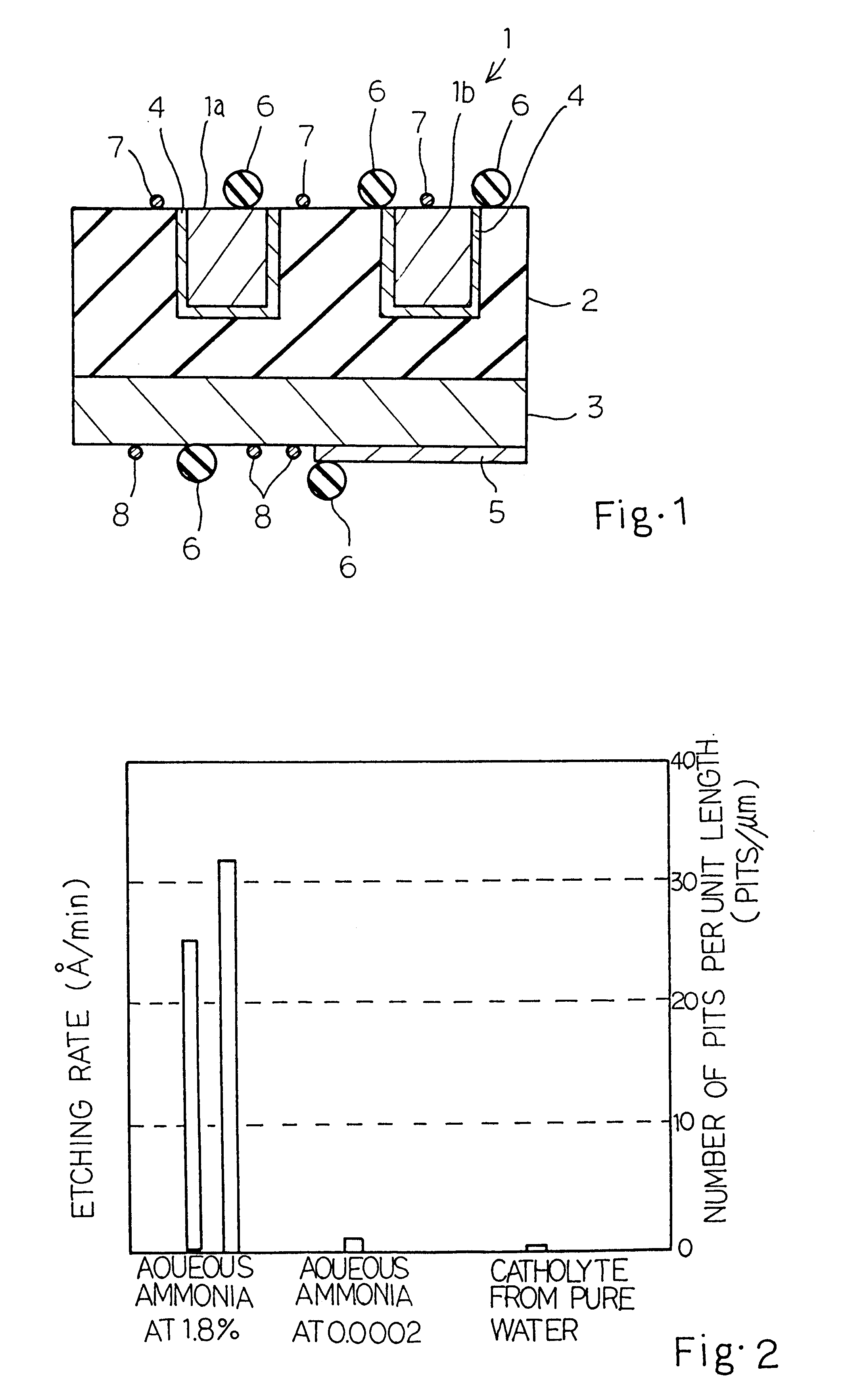
A silicon wafer was chemically mechanically polished, and the semiconductor structure shown in FIG. 1 was completed on the silicon wafer. Polishing slurry had been supplied to the surface to be polished during the chemical mechanical polishing, and contained alumina particles. Upon completion of the chemical mechanical polishing, the silicon wafer was transferred to the loader of the cleaning system for the underwater storage. The silicon wafer was moved to the first chamber of the cleaning system.

Using the rolling brushes 32, the alumina particles were brushed away from both surfaces of the silicon wafer, and the aqueous ammonia at 0.001 weight percent was supplied to both surfaces of the silicon wafer during the brushing. The brushing was continued for 20-60 seconds. After the brushing, the silicon wafer was rinsed in pure water for 5-20 seconds, and residual ammonia was removed from the surfaces of the silicon wafer.

Subsequently, the silicon wafer was moved to the second chamber,...

second example

A silicon wafer was chemically mechanically polished under the conditions same as the first example, and the semiconductor structure shown in FIG. 1 was completed on the silicon wafer. The silicon wafer was stored in the loader of the cleaning system, and was transferred to the first chamber.

Using the brushes 32, the alumina particles were brushed away from both surfaces of the silicon wafer, and catholyte was sprayed onto both surfaces during the brushing. The catholyte was obtained through the electrolysis of pure water, pH and the oxidation-reduction potential were 7.0 and -650 millivolts with the reference electrode of AgCl. Upon completion of the first cleaning, the silicon wafer was rinsed as similar to the first example.

The silicon wafer was transferred to the second chamber, and was subjected to the second cleaning under the conditions same as the first example. After the second cleaning, the silicon wafer was rinsed, and dried as similar to the silicon wafer in the first ex...

third example

A silicon wafer was chemically mechanically polished under the conditions same as the first example, and the semiconductor structure shown in figure 1 was completed on the silicon wafer. The silicon wafer was stored in the loader of the cleaning system, and was transferred to the first chamber.

Using the brushes 32, the alumina particles were brushed away from both surfaces of the silicon wafer under the conditions same as those in the first example. The silicon wafer was rinsed in the pure water, and was transferred to the second chamber.

The silicon wafer was subjected to the second cleaning under the same conditions except the washer sprayed on the major surface of the silicon wafer. The washer contained oxalic acid at 0.1 weight percent. After the second cleaning, the silicon wafer was rinsed and dried as similar to the silicon wafer in the first example.

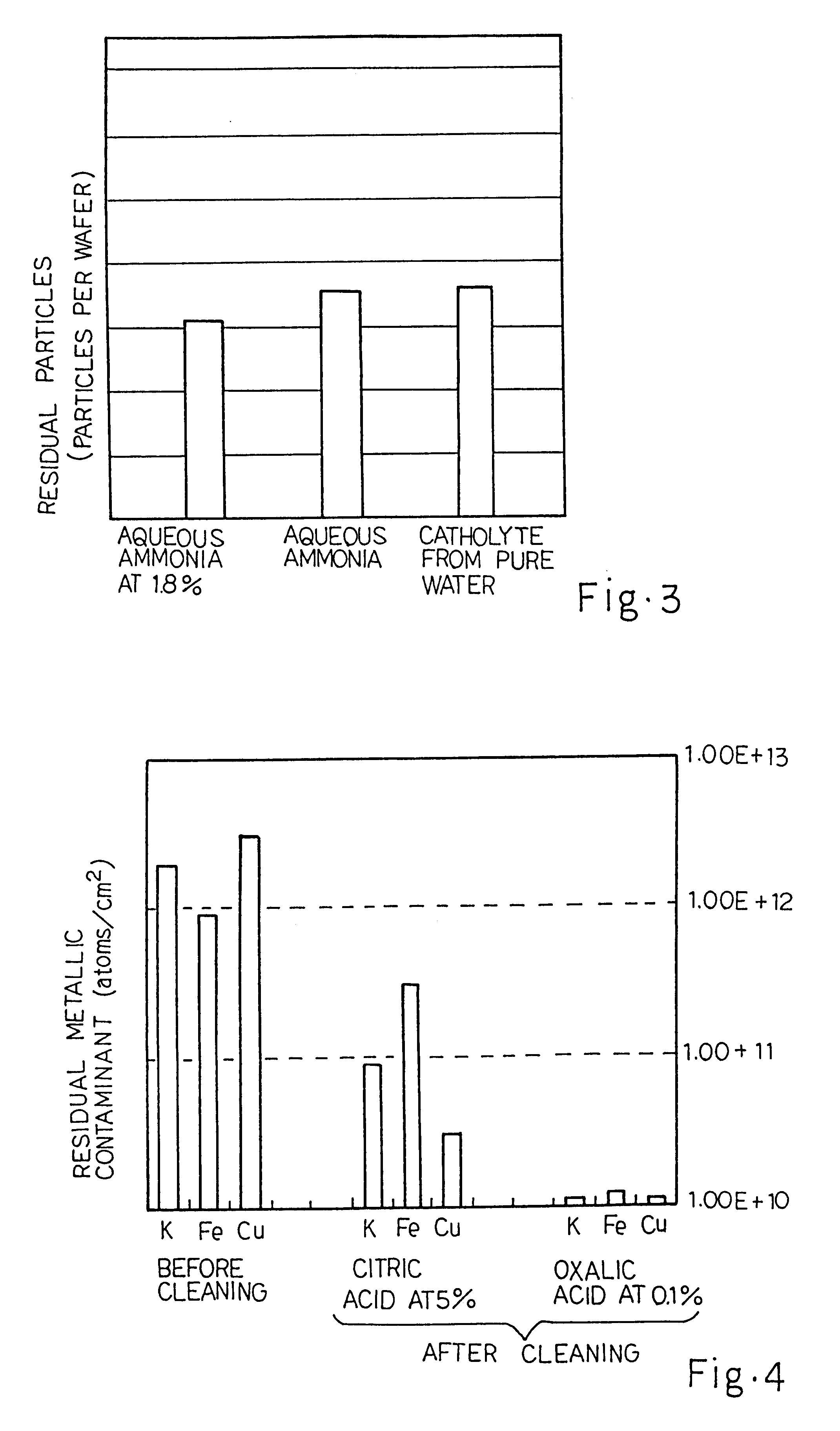
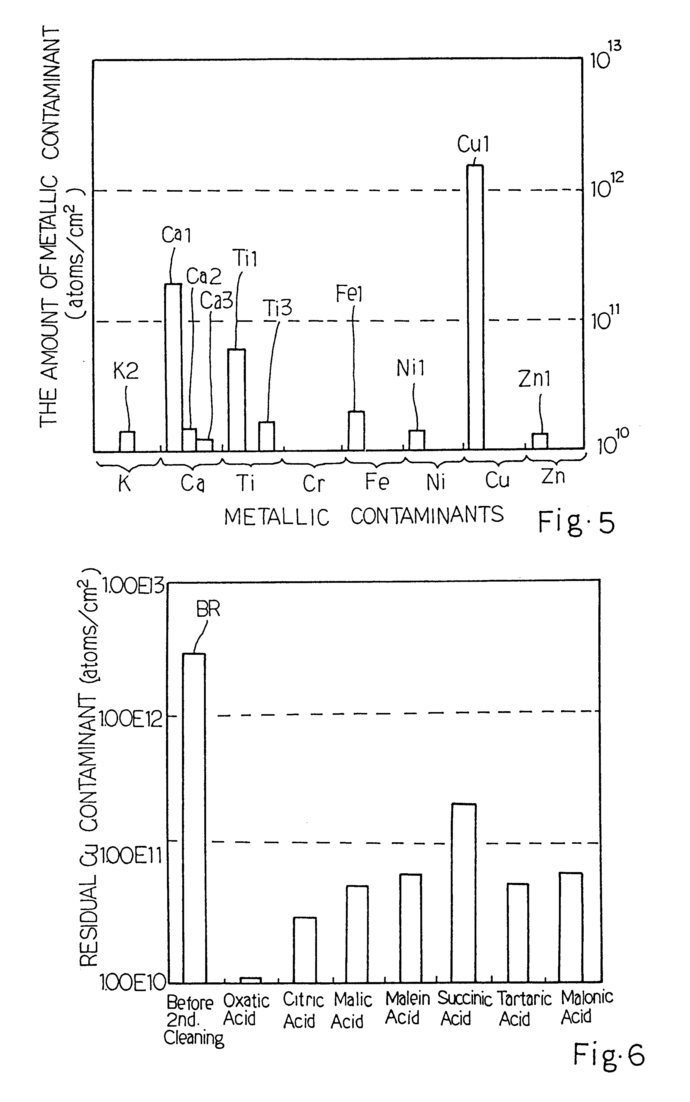
The present inventors confirmed that the alumina particles, the copper strip 5 and the metallic contaminants were removed from t...


PUM

PropertyMeasurementUnit
Fractionaaaaaaaaaa
Percent by massaaaaaaaaaa

Abstract

A copper wiring is desirable for a high-speed logic circuit integrated on a semiconductor substrate, and is patterned through a chemical mechanical polishing, wherein polishing particles are brushed away from the major surface of the resultant semiconductor structure by using hydrogen-containing water without damage to the copper wiring, and, thereafter, metallic contaminants such as copper is removed by using washer containing decontaminating agent selected from polycarboxylic acid, ammonium salts thereof and polyaminocarboxylic acid also without damage to the copper wiring.

Description

This invention relates to a wafer cleaning technology and, more particularly, to a method for cleaning a semiconductor wafer after a chemical mechanical polishing on a copper wiring.DESCRIPTION OF THE RELATED ARTOne of the technical goals for a semiconductor logic circuit device is a high-speed logic function. A copper wiring is attractive, because the electric resistance is low and the anti-electromigration property is good. The copper wiring is employed in the semiconductor logic circuit device. Although the copper wiring is desirable in view of the electric resistance and the anti-electromigration property, a copper layer is hardly patterned through a dry etching. The copper wiring is usually patterned as follows. First, a groove is formed in an insulating layer, and barrier metal such as titanium or tantalum and copper are successively deposited over the entire surface of the insulating layer. The entire surface of the insulating layer is covered with the barrier metal, and defi...

Claims


Application Information

Patent Timeline
IPC IPC(8): B08B3/08B24B37/04H01L21/02H01L21/306H01L21/321H01L21/3205H01L21/304H01L21/768H01L23/52H01L23/532
CPCB08B3/08B24B37/042H01L21/3212H01L21/0209H01L21/02074H01L21/304
Inventor AOKI, HIDEMITSUYAMASAKI, SHINYA
Owner RENESAS ELECTRONICS CORP
Why Eureka
Try Eureka