Semiconductor components, in particular photodetectors, light emitting diodes, optical modulators and waveguides with multilayer structures grown on silicon substrates

Inactive Publication Date: 2002-06-11
MAX PLANCK GESELLSCHAFT ZUR FOERDERUNG DER WISSENSCHAFTEN EV
View PDF10 Cites 384 Cited by
  • Summary
  • Abstract
  • Description
  • Claims
  • Application Information

AI Technical Summary

Problems solved by technology

However, substantial problems exist with such Si.sub.1-x Ge.sub.x /Si structures because Ge has a lattice constant which differs substantially from that of Si.
The mechanical strain which thereby results in structures of this kind makes it necessary to restrict the thickness of the layers to an extent which plac

Method used


Image

  • Semiconductor components, in particular photodetectors, light emitting diodes, optical modulators and waveguides with multilayer structures grown on silicon substrates
  • Semiconductor components, in particular photodetectors, light emitting diodes, optical modulators and waveguides with multilayer structures grown on silicon substrates
  • Semiconductor components, in particular photodetectors, light emitting diodes, optical modulators and waveguides with multilayer structures grown on silicon substrates

Examples


Embodiment Construction

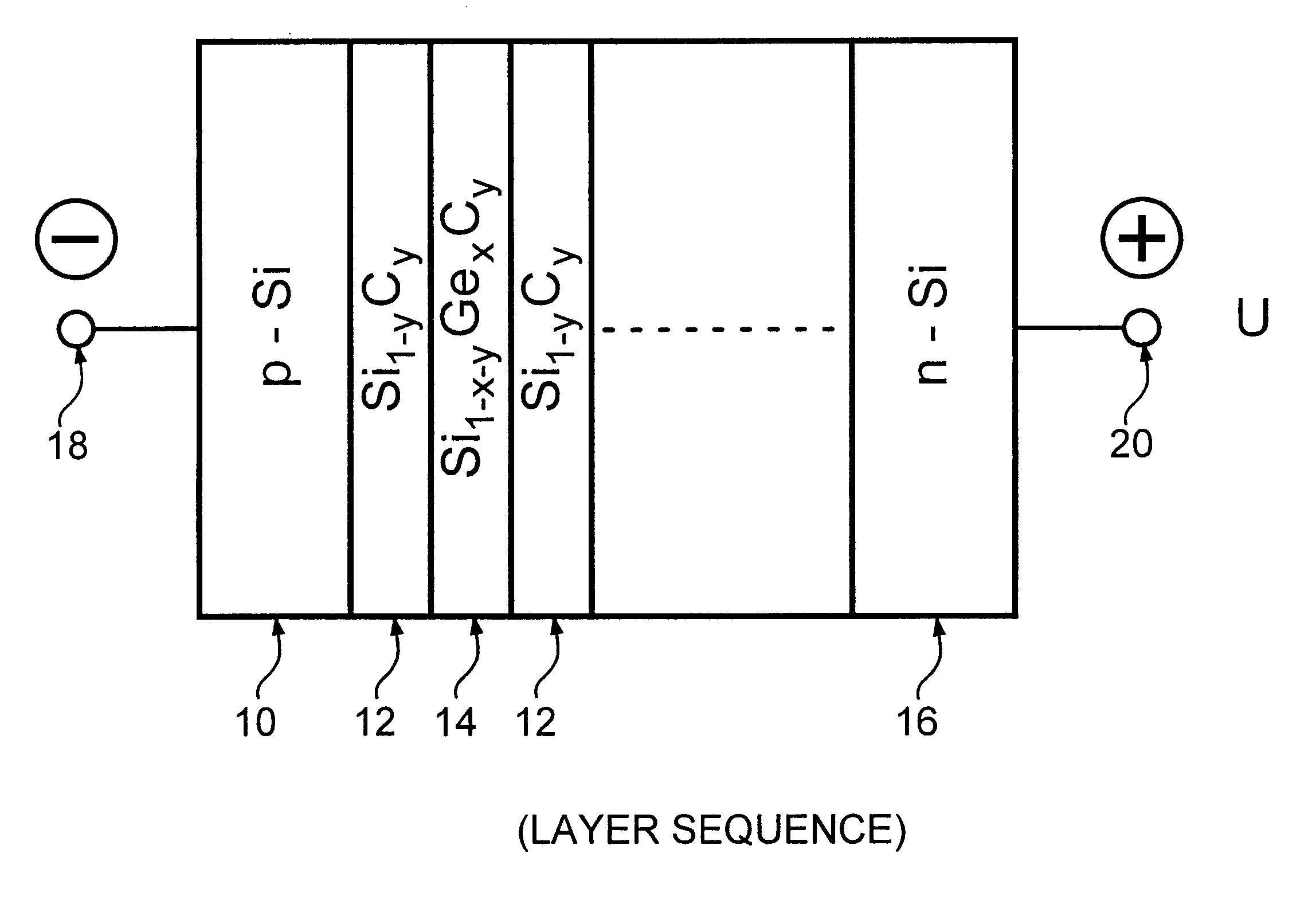
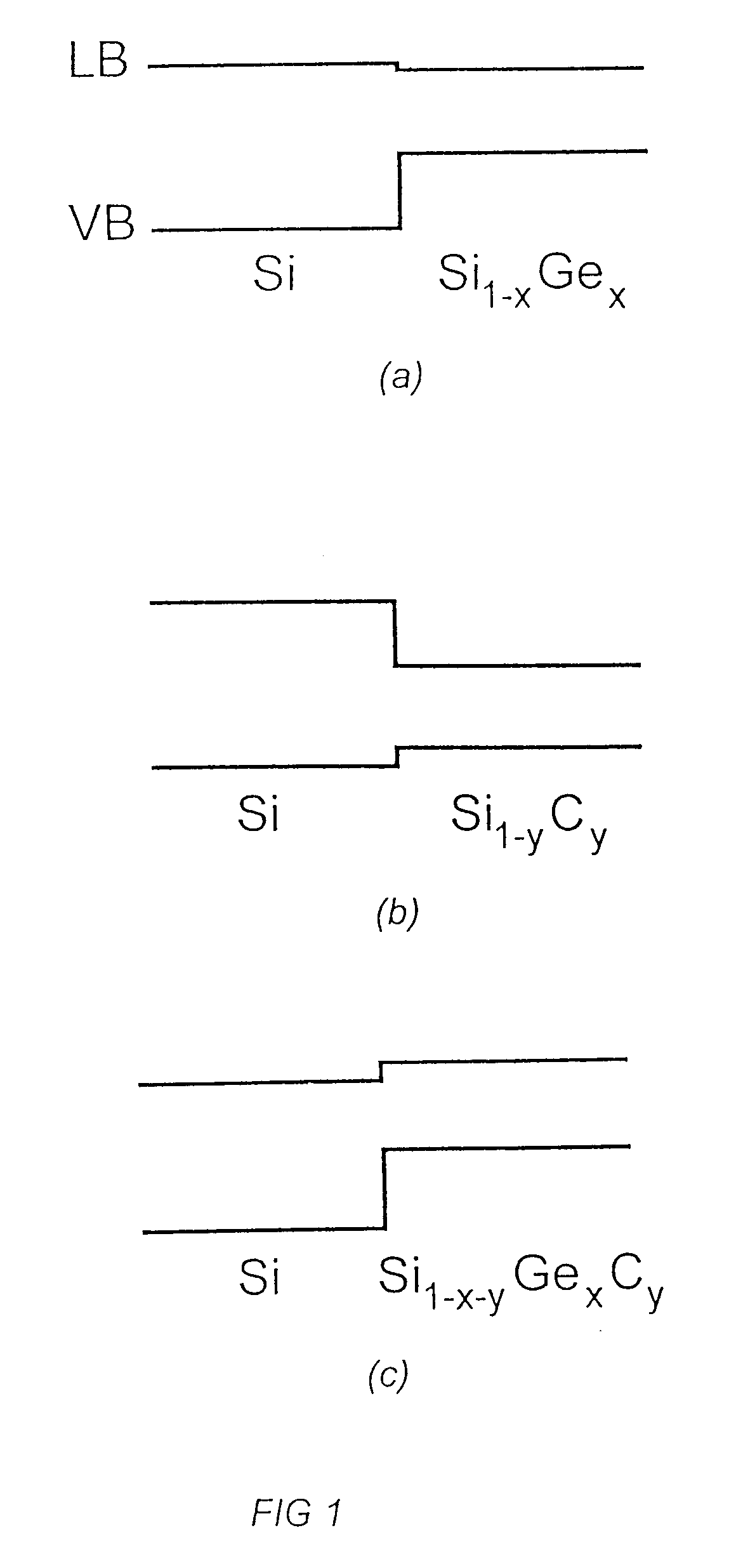
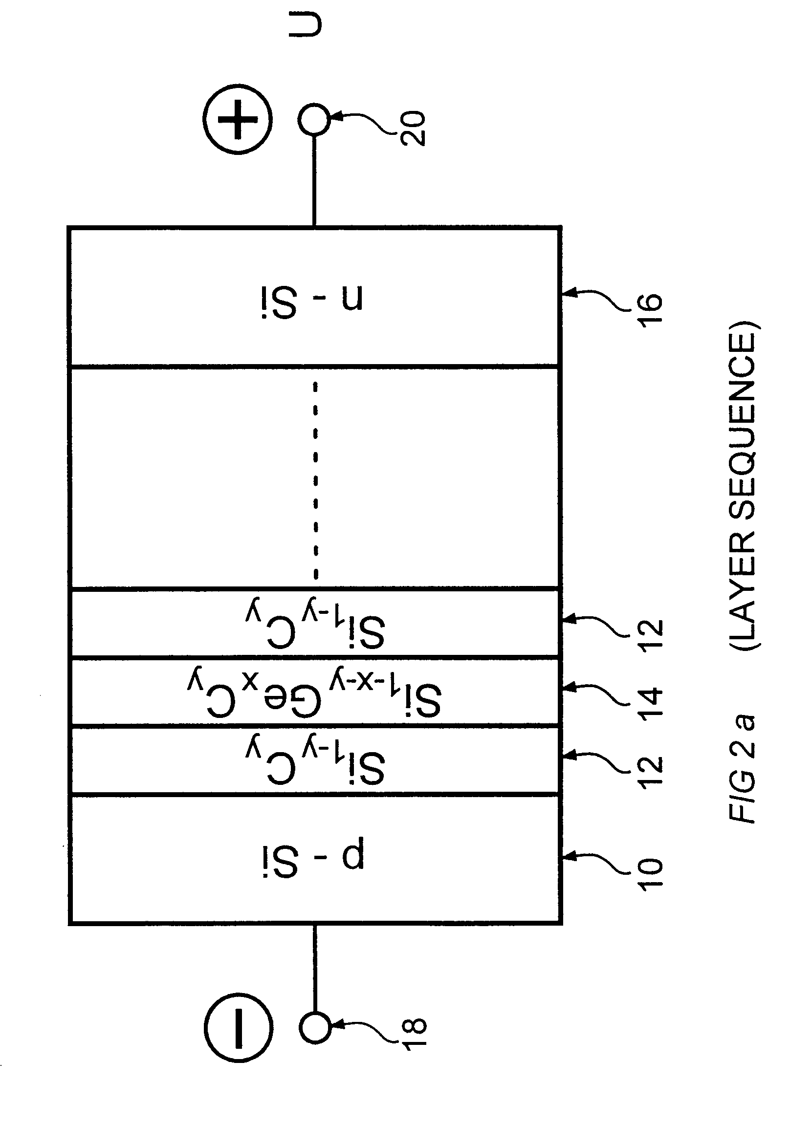
Turning first of all to FIG. 1a, the shape of the valence band VB and conduction band LB edges is shown for the transition from an Si single crystal substrate to a Si.sub.1-x Ge.sub.x alloy. It can be seen that the Si.sub.1-x Ge.sub.x alloy layers have a smaller band gap than Si and that the band edge step is mainly in the valence band.

FIG. 1b shows again the valence band VB and the conduction band LB for the transition from an Si single crystal substrate to an Si.sub.1-y C.sub.y alloy. It can be seen from this diagram that Si.sub.1-y C.sub.y alloy layers have a smaller band gap than Si and it is noted that the band edge step in Si / Si.sub.1-y C.sub.y heterostructures is mainly in the conduction band.

FIG. 1c shows the valence band VB and the conduction band LB for the transition from an Si single crystal substrate to a Si.sub.1-x-y Ge.sub.x C.sub.y alloy. Again the Si.sub.1-x-y Ge.sub.x C.sub.y alloy layers have a smaller band gap than Si. There is again a pronounced step in the vale...


PUM


Abstract

A semiconductor component, selected from the group comprising a photodetector, a light emitting diode, an optical modulator and a waveguide. The semiconductor component comprises an Si substrate, an active region formed on said substrate, and an Si capping layer on said active region. In one embodiment the active region is a superlattice comprising alternating layers of Si1-yCy and Si1-x-yGexCy, with the atomic fraction y of the Si1-x-yGexCy layers being equal to or different from the atomic fraction y of the Si1-yCy layers. In another embodiment it is a superlattice comprising a plurality of periods of a three-layer structure comprising Si, Si1-yCy and Si1-xGex layers. In a third embodiment it is a superlattice comprising a plurality of periods of a three-layer structure comprising Si, Si1-yCy and Si1-x-yGexCy layers, with the atomic fraction y of the Si1-x-yGexCy layers being equal to or different from the atomic fraction y of the Si1-yCy layers. The components have faborable optical and electrical properties and are suitable for integration on a Si substrate.

Description

Photodetectors and light emitting diodes (LEDs) in the wavelength range from 1.55 to 1.3 .mu.m are used in telecommunication by means of glass fibers. At present, use is principally made of components based on III-V semiconductors which are relatively expensive.DESCRIPTION OF PRIOR ARTSome proposals have been made relating to Si.sub.1-x Ge.sub.x / Si semiconductor components for use in this wavelength range and have been reported by H. Presting et al. in Semiconductor Science Technology 7, pages 1127 and sequel of 1992 and in App. Phys. Lett., Vol. 66 No. 17, Apr. 24, 1995 in the article "Strained Si.sub.1-x Ge.sub.x multi-quantum well waveguide structure on (110) Si" by K. Bernhard Hofer, A. Zrenner, J. Brunner and G. Abstreiter.However, substantial problems exist with such Si.sub.1-x Ge.sub.x / Si structures because Ge has a lattice constant which differs substantially from that of Si. The mechanical strain which thereby results in structures of this kind makes it necessary to restr...

Claims


Application Information

Patent Timeline
IPC IPC(8): G02F1/017G02F1/01H01L29/02H01L29/15H01L31/0352H01L31/0248H01L33/00H01L33/06H01L33/34
CPCB82Y20/00G02F1/017H01L33/34H01L31/035254H01L33/06H01L29/155
Inventor BRUNNER, KARLEBERL, KARL
Owner MAX PLANCK GESELLSCHAFT ZUR FOERDERUNG DER WISSENSCHAFTEN EV
Why Eureka
Try Eureka