Laminate-based apparatus and method of fabrication

a technology which is applied in the field of laminate-based apparatus and fabrication method, can solve the problems of limiting the repeatability of performance, undesirable variability, and individual devices produced by such a "assembly-line" type process, and generally having relatively complex structures

Inactive Publication Date: 2002-06-25
TELEDYNE
View PDF27 Cites 132 Cited by
  • Summary
  • Abstract
  • Description
  • Claims
  • Application Information

AI Technical Summary

Problems solved by technology

The individual devices produced by such an "assembly-line" type process generally have relatively complicated structures and exhibit high unit-to-unit variability.
Such variability is undesirable because it limits the repeatability of performance from unit-to-unit.
In particular, in the case of relays used to switch high frequency signals, such variances in physical geometry may result in changes in the device's inductance and capacitance, rendering such a device undesirable.
While conventional electromechanical relays can be designed to reduce unit-to-unit variability, the resultant device is typically more costly to manufacture.
Combined, these shortcomings render such conventional electromechanical relay devices undesirable.
However, MEMS fabrication techniques are not without their drawbacks.
In the example of electromechanical relays, the physical properties of the silicon, quartz, and glass substrates on which the MEMS relay devices are typically fabricated are not well suited in general to the demands placed on them by the design of an electromechanical relay.
Due to the reduced scale of MEMS devices, and the materials and processes used in MEMS fabrication, MEMS devices do not easily lend themselves to vertical processing.
Accordingly, the physical spacing, and thus the signal isolation, between the contacts in a MEMS relay is often insufficient to fully isolate the contacts when the relay is in the open position.
Thus, MEMS relays often exhibit an unacceptable flow of current across the contacts when the relays are in the open position.
This problem is particularly apparent when the relays are used to switch high frequency signals.
Silicon, for example, has a relatively high microwave loss tangent, thereby limiting the performance at high frequencies of devices formed from silicon.
Such variations in impedance at the transition points between the various structures of the relay (typically called "mismatches") can adversely affect performance of the relay at certain frequencies.
For example, over a given range of frequencies, a mismatch may cause the signal carried by the relay to become attenuated and / or the waveform of the signal to become distorted, thus rendering the relay unsuitable for certain applications.
However, MEMS devices may be fabricated on only a limited number of substrate materials.
As previously noted, such materials often exhibit unacceptable performance characteristics when used in devices designed to function at high frequencies.
Thus, such devices often require additional or secondary packaging to overcome these shortcomings in performance.
The need for secondary packaging represents a significant disadvantage to the use of MEMS fabrication techniques in relay applications.
This secondary packaging step is highly undesirable due to the additional cost of the lead frame and packaging step, such cost will often exceed the cost of the relay itself.
In addition, the potential yield loss in the resulting packaged device and the potential performance limitations that may result in the packaged device due to the creation of impedance mismatches between the device and the package are also quite undesirable.

Method used


Image

  • Laminate-based apparatus and method of fabrication
  • Laminate-based apparatus and method of fabrication
  • Laminate-based apparatus and method of fabrication

Examples


Embodiment Construction

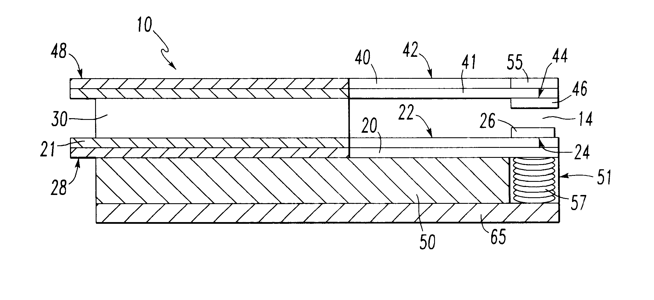
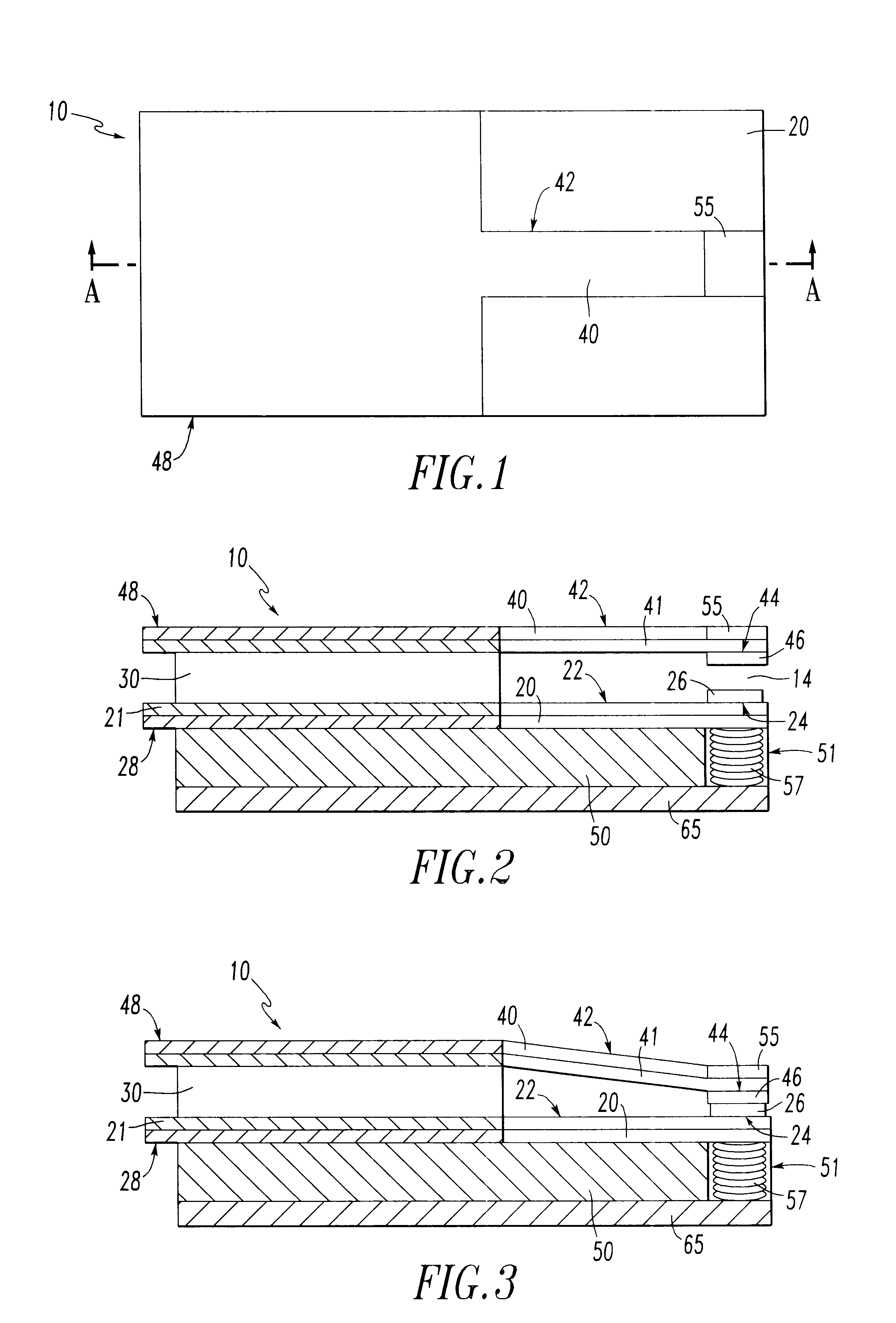
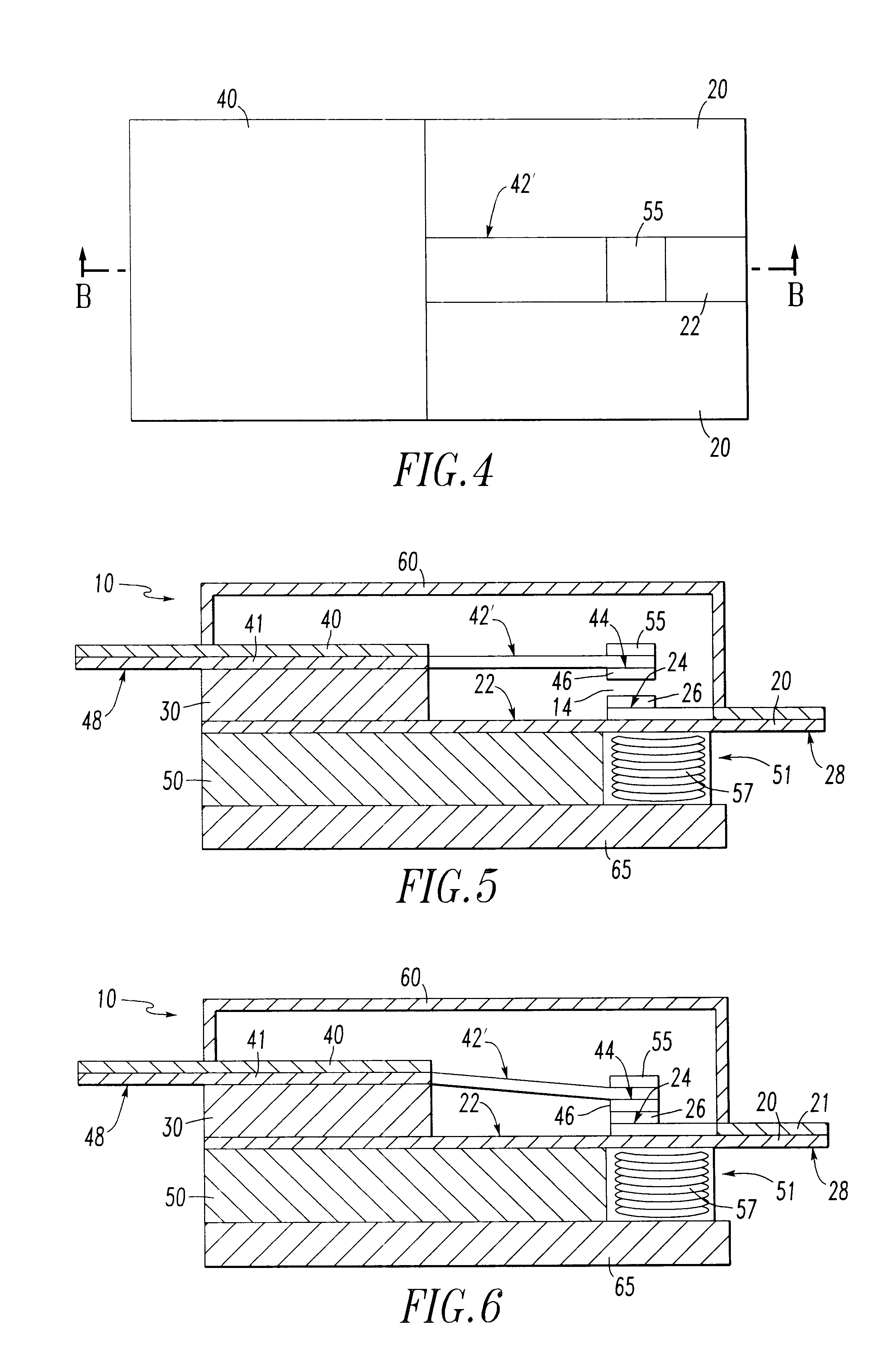
Referring now to the drawings for the purposes of illustrating embodiments of the invention only, and not for purposes of limiting the same, the Figures show various laminate-based electromechanical relay devices, fabricated according to the method of present invention from layers of dielectric material laminated together to form a unitary three-dimensional electromechanical structure. While the present laminate based. fabrication method may, for example, permit the straight forward fabrication of electromechanical relay devices that are optimized to function as controlled impedance structures at microwave frequencies, such as, those shown herein in the Figures, one of average and ordinary skill in the art will appreciate that the present invention may be successfully employed to fabricate myriad of other electromechanical devices. Therefore, it will further be appreciated that the laminate-based electromechanical relay devices referred to herein in the Figures and in the following ...


PUM

PropertyMeasurementUnit
electrically conductiveaaaaaaaaaa
photo resistanceaaaaaaaaaa
magneticaaaaaaaaaa

Abstract

The present invention discloses a laminate-based electromechanical device and a method of fabricating laminate-based electromechanical devices. The device includes two or more layers of laminate bonded together to form a unitary laminate structure. The layers of laminate include a layer of organic dielectric material that may have at least a portion of one layer of electrically conductive material adherent thereto. The layers of organic dielectric material are bonded to form a unitary laminate structure through a process of lamination. The structures that make up the electromechanical device may be formed either before or after bonding. In particular, the various electromechanical structures that make up the electromechanical device are formed from the layers of organic dielectric material and the layers of electrically conductive material adherent thereto using a predetermined sequence of additive and subtractive fabrication techniques.

Description

Not ApplicableFEDERALLY SPONSORED RESEARCHNot ApplicableTECHNICAL FIELD AND INDUSTRIAL APPLICABILITY OF THE INVENTIONThe present invention relates to electromechanical devices having laminate structures and methods for fabricating such devices. More particularly, the present invention relates to laminate-based electromechanical relay devices and methods for fabricating such relays. However, the present laminate-based fabrication method may be suitably adapted for use in connection with the design and fabrication of a wide variety of laminate-based electromechanical devices. Accordingly, an example of a possible application of the laminate-based fabrication method and apparatus of the present invention includes the design and fabrication of high frequency range electromechanical relay devices.DESCRIPTION OF THE INVENTION BACKGROUNDConventional electromechanical devices, such as electromechanical relays, have traditionally been fabricated one individual device at a time, by either man...

Claims


Application Information

Patent Timeline
Patent Type & Authority Patents(United States)
IPC IPC(8): H01H50/00H01H1/00H01H49/00
CPCH01H50/005H01H1/0036H01H49/00Y10T29/49204Y10T29/49105Y10T29/49117H01H2001/0073
Inventor STEENBERGE, ROBERT W.
Owner TELEDYNE
Why Eureka
Try Eureka