Method of manufacturing a semiconductor device utilizing a laser annealing process

a laser annealing and semiconductor technology, applied in semiconductor lasers, manufacturing tools, instruments, etc., can solve the problems of affecting the quality of semiconductor devices,

Inactive Publication Date: 2002-08-27
SEMICON ENERGY LAB CO LTD
View PDF103 Cites 48 Cited by
  • Summary
  • Abstract
  • Description
  • Claims
  • Application Information

AI Technical Summary

Problems solved by technology

However, conditions for laser annealing are not yet established because conventional laser annealing processes were each conducted independently under differing conditions which depend upon the apparatuses and the coating conditions chosen individually in each process.
This has misled and has allowed many to think that the laser annealing technology fails to give results reliable and consistent enough to make the process practically feasible.
In a process for fabricating a semiconductor device, a deposition film is considerably damaged by processing such as ion irradiation, ion implantation, and ion doping, and is thereby impaired in crystallinity as to yield an amorphous phase or a like state which is far from being called as a semiconductor.
However, in a film containing boron as an impurity, the film undergoes degradation by the irradiation of a laser of such a high energy density.
However, this is not true because it was found that the morphology of the coating deteriorates with increasing number of shots to increase fluctuations in a microscopic level.

Method used


Image

  • Method of manufacturing a semiconductor device utilizing a laser annealing process
  • Method of manufacturing a semiconductor device utilizing a laser annealing process
  • Method of manufacturing a semiconductor device utilizing a laser annealing process

Examples


Embodiment Construction

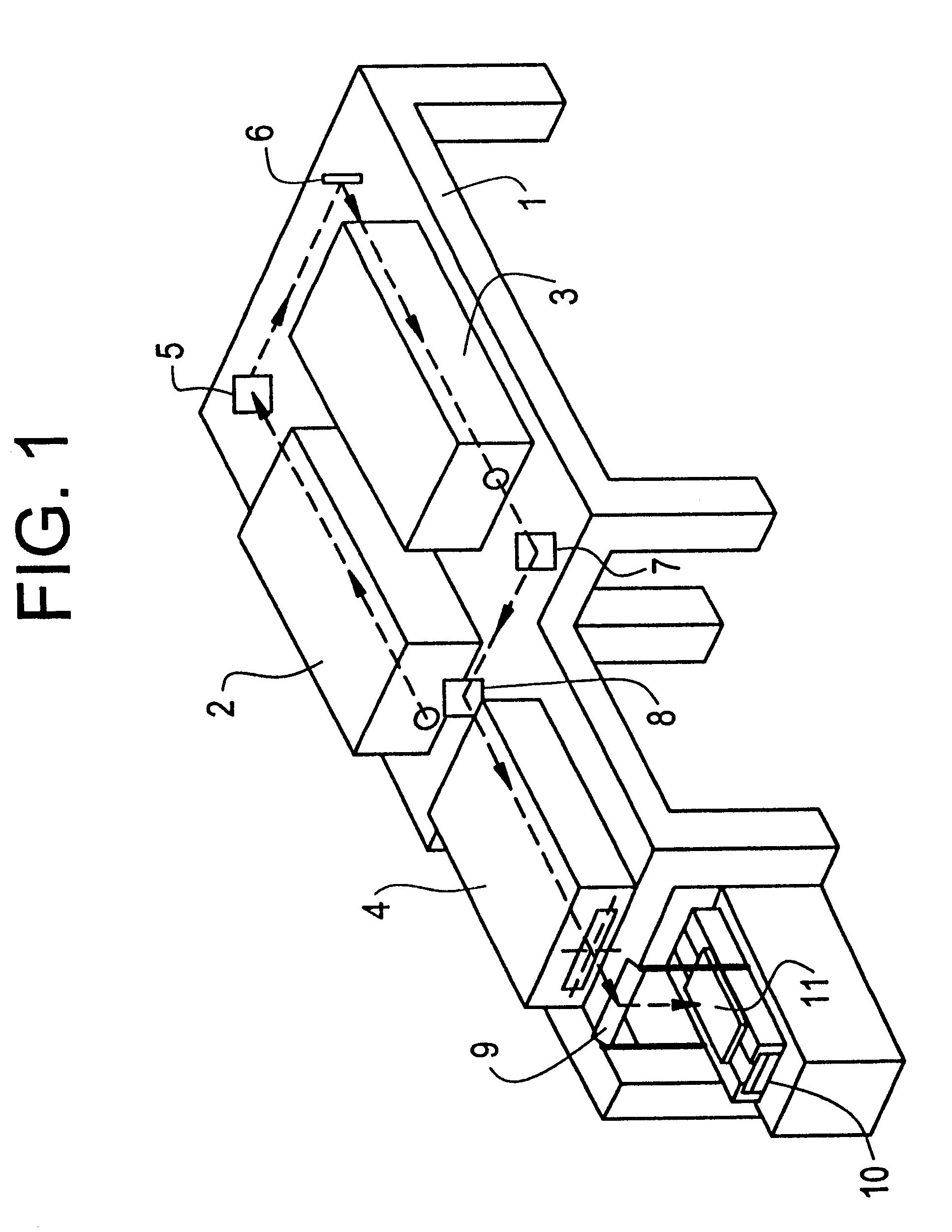
In this EXAMPLE, an impurity is introduced into a film comprising a Group IV element for imparting one of N-type conductivity and P-type conductivity thereto, and another impurity is introduced into a portion of the film with a mask for imparting the other one of the N-type conductivity and P-type conductivity to said portion. In FIG. 1 is shown schematically a laser annealing apparatus having used in the present example. A laser beam is generated in a generator 2, amplified in an amplifier 3 after traveling through full reflection mirrors 5 and 6, and then introduced in an optical system 4 after passing through full reflection mirrors 7 and 8. The initial laser beam has a rectangular beam area of about 3.times.2 cm.sup.2, but is processed into a long beam having a length of from about 10 to 30 cm and a width of from about 0.1 to 1 cm by the optical system 4. The maximum energy of the laser having passed through this optical system was 1,000 mJ / shot.

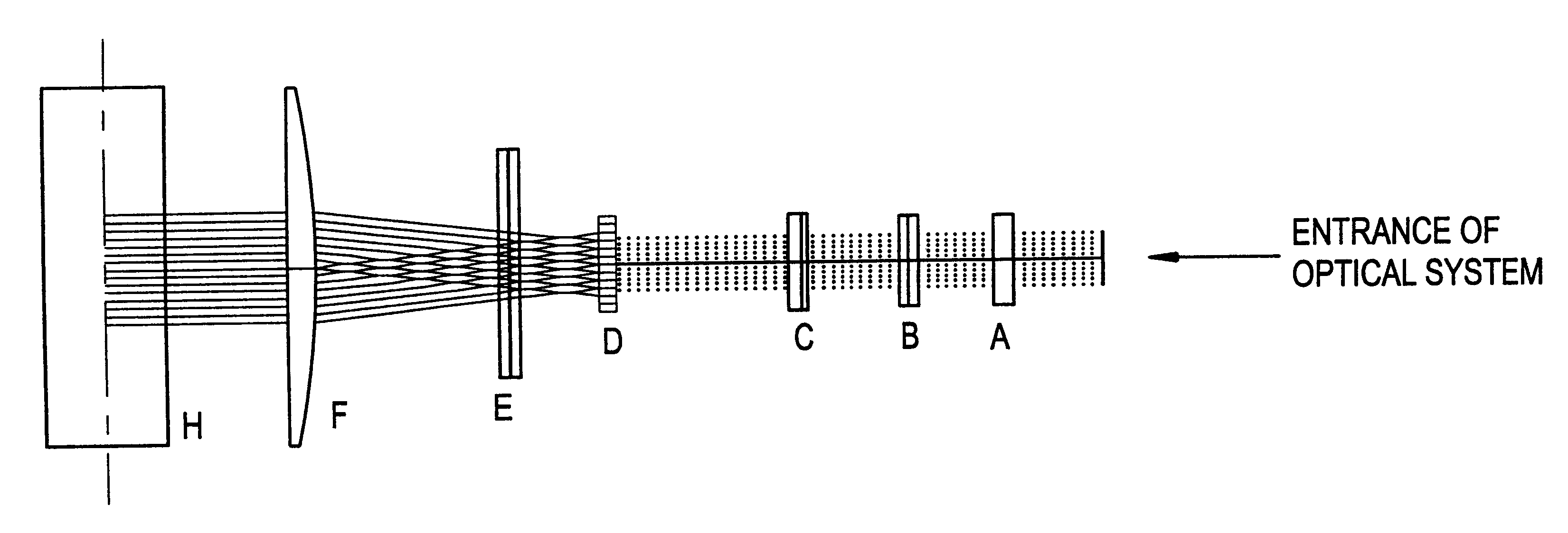
An optical path in the optical sy...


PUM

PropertyMeasurementUnit
widthaaaaaaaaaa
widthaaaaaaaaaa
lengthaaaaaaaaaa

Abstract

A laser annealing process for recovering crystallinity of a deposited semiconductor film such as of silicon which had undergone morphological damage, said process comprising activating the semiconductor by irradiating a pulsed laser beam operating at a wavelength of 400 nm or less and at a pulse width of 50 nsec or less onto the surface of the film, wherein,said deposited film is coated with a transparent film such as a silicon oxide film at a thickness of from 3 to 300 nm, and the laser beam incident to said coating is applied at an energy density E (mJ/cm2) provided that it satisfies the relation:where N is the number of shots of the pulsed laser beam.

Description

1. Field of the InventionThe present invention relates to a highly reliable, laser annealing process suited for use in mass production of semiconductor devices, which enables uniform annealing at high yield. More particularly, the present invention provides a laser annealing process of a deposited film whose crystallinity had been greatly impaired by the damage it had received through processes such as ion irradiation, ion implantation, and ion doping.2. Prior ArtAt present, methods of lowering of process temperatures in fabricating semiconductor devices are extensively studied. The reason for such an active research for low temperature processes owe partly to the need for fabricating semiconductor elements on an insulator substrate made of, e.g., glass. Laser annealing technology is regarded promising as the ultimate low temperature process.However, conditions for laser annealing are not yet established because conventional laser annealing processes were each conducted independentl...

Claims


Application Information

Patent Timeline
Patent Type & Authority Patents(United States)
IPC IPC(8): C23C14/58C23C16/56H01L21/20H01L21/02B23K26/067B23K101/40G02B13/00G02B27/09G02F1/00G02F1/35H01L21/00H01L21/26H01L21/265H01L21/268H01L21/322H01L21/324H01S3/00H01S3/09H01S3/097H01S5/024
CPCC23C14/58C23C14/5813C23C16/56G02B27/09G02B27/0966H01L21/2026H01L21/26513H01L21/268H01L27/1285H01L21/2022H01L21/84H01L21/02422H01L21/02532H01L21/02678H01L21/02686
Inventor YAMAZAKI, SHUNPEIZHANG, HONGYONGISHIHARA, HIROAKI
Owner SEMICON ENERGY LAB CO LTD
Why Eureka
Try Eureka